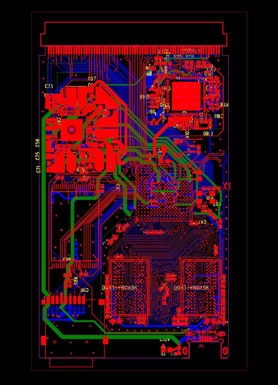
5 Aug 2014: Planes completed
Plane areas and copper have now been completed: most visible is the areas in solid red surrounding the AXP223 in the top left corner. A few schematics corrections had to be made on the Power routing at this late phase, meaning that the connectivity is not as "beautiful" as it could be, however it should be perfectly functional. The final phase will be to flood the planes and correct any non-connectivity errors.

31 Jul 2014: Main routing completed
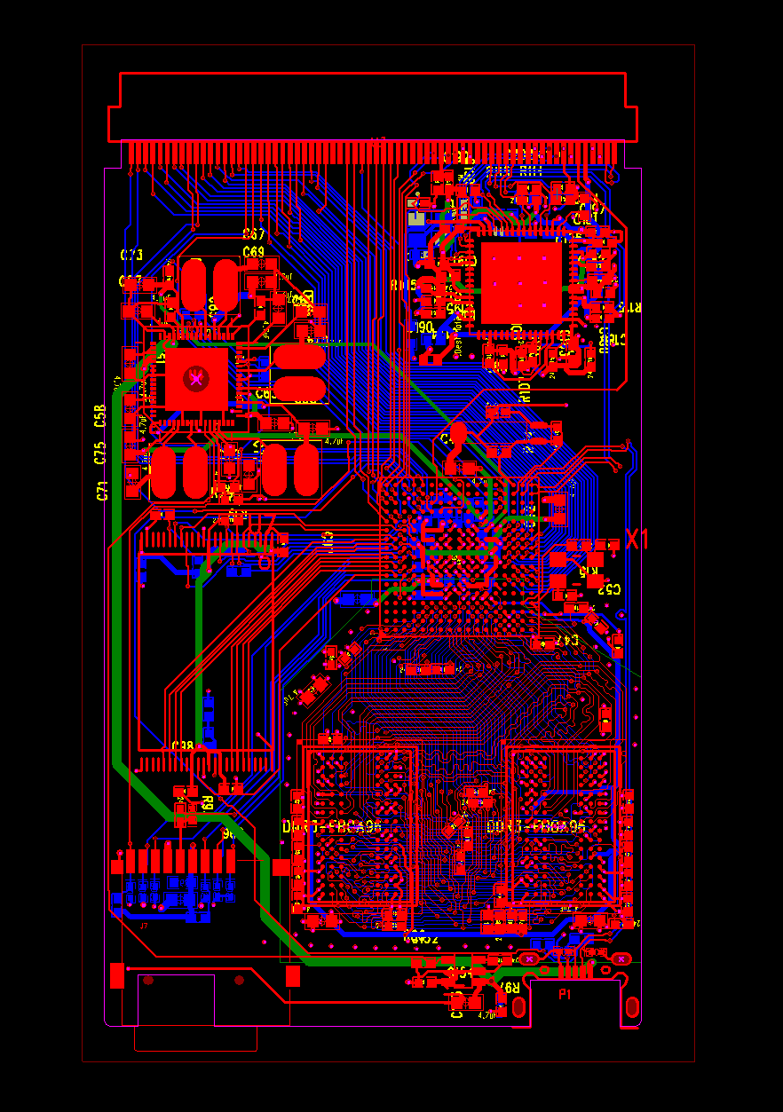
The main GPIO and other routing is now completed, leaving just the power planes to do. It is noted that the pinouts for the A33 have been designed very carefully: note that the majority of the NAND pinouts go directly on a single layer between the CPU and the TSOP-48 NAND IC (left middle: red lines). Likewise the RGB/TTL BGA pin placement has been extremely well thought-out, so that the tracks in blue (to top left corner) could likely be done almost with very little cross-over. However, as long as this layout is functional it need not be fine-tuned to such an extent. It's quite exciting that this PCB is progressing so rapidly!

30 Jul 2014: Component Placement completed
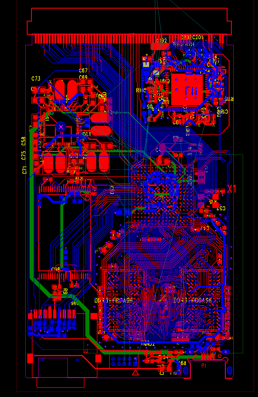
With some re-use from other PCBs using the SMC 9514 this board is rapidly approaching completion. Top-right is the SMC 9514. Middle-right is the Allwinner A33, and below it are two 1GByte 16-bit DDR3 RAM ICs. Below that (bottom right) is a mid-mount Micro USB-OTG. Bottom left is a Micro-SD card slot. Above that is one TSSOP-48 NAND IC. Top left is the AXP223 PMIC. This board is really very simple. It is also a 4-layer PCB so cost will be reduced here.

27 Jul 2014: Preliminary PCB layout
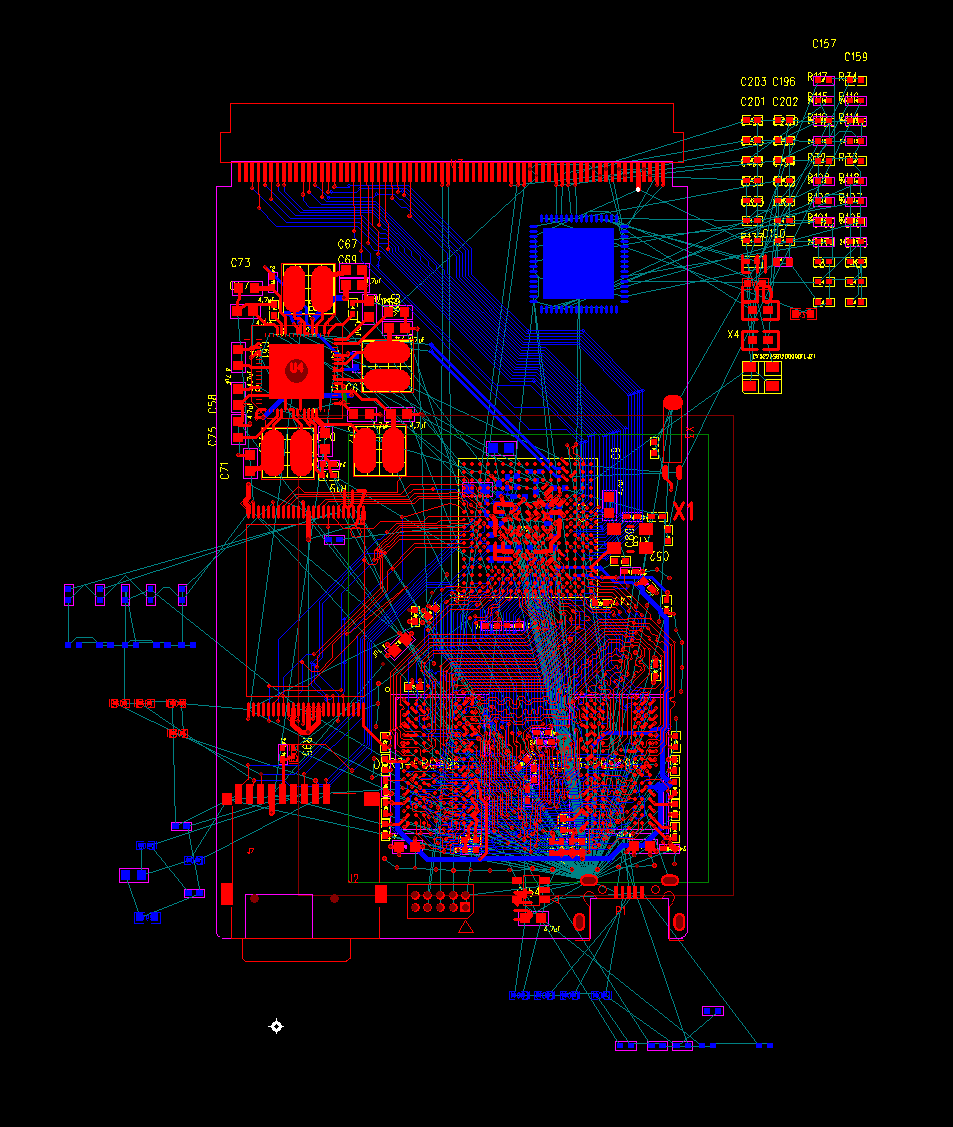
Thanks to Wits-Tech and Allwinner for the comprehensive documentation, as well as the PCB files with the DDR3 RAM layout already completed. Thanks to that assistance, and re-using many parts and circuits from other CPU Cards the A33 PCB has been brought to this 40% completed phase within one day:
