A Transmission Line Taper of Improved Design, R. W. Klopfenstein, 1956
In which, finally, action can be taken to finish the HDMI track layout. This update will describe why it is necessary to create an extraordinarily-complex taper (so as to prevent signal-bounce basically), and go into detail on how that's being done. Summary: It's sufficiently complex to do the layout that it's actually worthwhile to export the PCB file to an ASCII format, write a parser for the proprietary format, and add a viewer, then modify the tracks using a computer algorithm.
So, Richard referenced this amazing paper from 1956, which has had some minor corrections from another paper published in 1973, but otherwise this is something that I simply haven't seen - anywhere - in any recommended CAD Design practices, anywhere. When you get down to the details it is hardly surprising: normally these practices would only be applied at very high frequency (microwave), but in this case we are being extra paranoid, not least because prior revisions of the HDMI layout failed to provide a proper high-quality stable signal: artefacts cropping into the HDMI output that basically wrecked any chance of signing off on that particular board for production purposes.
The purpose of Klopfenstein's approach, which is outlined in an article online here https://www.microwaves101.com/encyclopedias/klopfenstein-taper is to create a smooth transition between impedances on a track. Imagine a water pipe doing down from a 1in to a 0.5in bore, and expecting to get laminar flow https://en.wikipedia.org/wiki/Laminar_flow - no chance, right? Water isn't quite the same as electricity but the analogy gives you the general idea. Electrical current has something called "impedance" - it's electro-magnetic resistance - and the resistance is related directly to the thickness of the copper and also how close a track is to "ground" (and also to other signals).
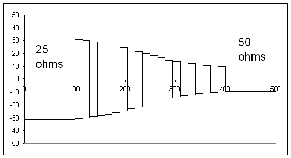
In the Microwaves 101 article it goes into detail on how a Klopfenstein taper can be emulated by a series of staggered steps, and it turns out that doing so isn't half bad. In effect you treat the track as a series of gradually-changing (very short) resistors. The advantage of a series of staggered steps is, you can use a discrete computer algorithm to do the maths, instead of having to do complex partial linear equation solving and so on. Here's what a staggered taper would look like if you were reducing a track width equivalent to 25 ohms up to 50 ohms impedance:
However we're not going to apply this technique to the actual tracks: the tracks will remain at 5 mil (5 thousandths of an inch). What instead we're going to do is change the impedance by changing the gaps between tracks and Ground, applying the exact same Klopfenstein technique. Why change the size of the gaps, not the track width? Well, the minimum track width and track-to-track clearance to ensure that the PCB manufacturing is not horrendously expensive is around 5 mil. So instead we are changing the impedance by increasing the distance to the Ground plane. Bear in mind: HDMI rules require that the differential pair impedance be 100 ohms, and that the tracks themselves (as a single track, known as "single-ended") be 50 ohms. More on these rules can be found here: https://ez.analog.com/docs/DOC-11303 where the key differences that we have between the example layout given there are firstly that all four tracks have to immediately undergo a big group right-angle turn; second that there's not enough space to keep them on a single layer, and third that we're using a Micro-HDMI connector Type D not a standard full-sized HDMI Type A. Interestingly, not included in that article, but found on other sites including TI's HDMI layout recommendations, it's considered generally a good idea to deliberately introduce a small delay into the CLK differential pair. We are extremely fortunate that, on the group 90 degree turn, the HDMI CLK pair is on the outside, making it automatically the longest.
So if I remember correctly from the figures that I gave him, Richard had kindly calculated that the differential-pair impedance was something like 110 ohms, which is close enough to be acceptable, and that the single-ended impedance was 70 ohms, which is just within acceptable bounds. He also kindly calculated that we need to keep a separation gap between pairs and also the surrounding flood-fill of GND of 15mil.
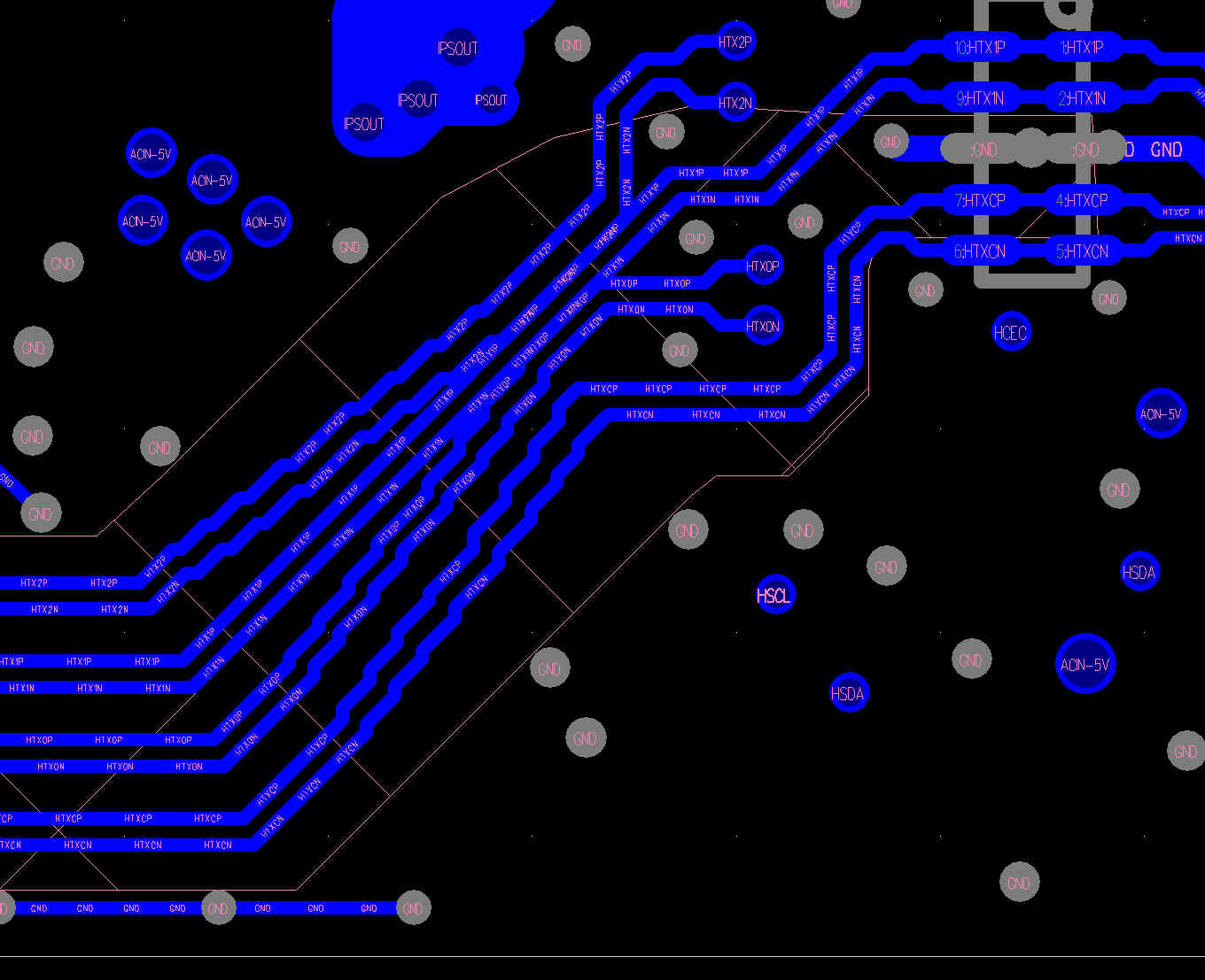
Here's the crux of the problem: at the beginning and the end it is impossible to keep 15 mil between pairs. It's barely possible to get a 5 mil signal out between two of the BGA pads and still keep a 5 mil clearance, let alone attempt a 15mil one.
So at some point, the distance between pairs - as well as the distance to the GND flood-fill - has to drop from 15 mil down to 5 mil, and that's precisely where you cannot just go "spangggg", I fink I will make the distance to GND be 5 mil now, because, just as if you were doing a track going from 15 mil down to 5 mil, if you drop the spacing down in a harsh fashion you completely waste all the effort of having done a nice layout of the rest of the differential pairings (which took several weeks to get right). Basically, any harsh transitions result in signals bouncing back down the line. If the signal bounces back down the line, it bounces again at the other end, combining with the next one that's currently being generated by the HDMI transmitter (the processor), and that's basically why we had awful noise on the display of previous revisions of the EOMA68-A20 PCB.
So, the first thing is: we need to design a smooth transition taper that narrows down the GND impedance, and the second thing is: Richard kindly provided a table based on Klopfenstein's original 1956 paper using the "stepping" technique outlined in the first article, above, which does exactly that. All that's left, now, is to actually implement those transitions. There are 80 separate and distinct points that need to be added. There is absolutely no way in hell that I am doing those by hand, and that's where a bit of python programming comes in.
Automatically creating the Klopfenstein taper in python
So, I'm using a proprietary PCB CAD program. I did try using KiCAD: i fought with it and, I am reluctant to have to point out that several of us fought with an extremely transigent attitude of the KiCAD developers for many months, until I gave up with the realisation that for such a complex board where there are not even any one-way converters let alone two-way, proprietary PCB CAD software was the only realistic way to get this board done.
This PCB software simply does not have anything remotely resembling a useable programming interface for this type of task. I took a look at the COM interface: much of what is needed is read-only. It's also hopelessly undocumented anyway. So the only remaining approach - one that I've considered doing for quite some time - was:
- To export a partly-finished PCB CAD layout to ASCII format
- Write a parser for the track layout (just the relevant tracks)
- Write a "display" program that would at least mean I didn't have to re-insert the tracks back into the proprietary program followed by import at last just to see what they looked like
- Write some code that modifies the tracks according to the Klopfenstein taper table
Rather than write code which inserts the actual tracks themselves, what I decided to do instead was to add the 80 points manually in an approximation of the taper, followed by modifying them in-situ. Here's the approximation, which the program will need to adjust to look more like the taper above:
So the first phase was to write a parser. I decided to use python-ply, starting from the BASIC interpreter example, and quickly came up with something that understood the ASCII format of the PCB track layout. It's a little weird, as spaces are actually part of the file-format. During the parsing phase I got each "class" representing sub-sections of the file to actually output the exact same text, not just to be able to compare it with the original but also to ensure that when it comes to modifying then outputting the points I have a way to actually generate the required sections in the original proprietary ASCII file-format.
The second phase was to track down an example "display" system, and for that I found python-pygame. Of course, one of the subsystems of pygame is borked (the sound mixer thread hangs), as a really really obscure stackexchange report showed. So by only calling pygame.display.init() and pygame.font.init() i.e. only initialising those subsystems that are actually needed, I was able to work around that problem as well. The third problem turns out to be that pygame line drawing isn't properly drawing lines of an actual required width. Yet another search turned up a recipe on stackexchange for using anti-aliased rectangle and flood-fill to create proper line segments, and ta-daaa, we have an approximation of the traces sufficient to actually see what's going on, and experiment within tens of seconds as opposed to minutes by being forced to import into a proprietary program by hand.
Note that there's no arcs on the tracks, at the corners where the track changes direction, and that's ok: all that's needed is an approximation. Also note that where, in the original PCB CAD program, I had put in "arcs" into the track at various points, the "point" represents the centre of the circle, so the track jumps weirdly where there should be an arc instead. I had no idea what I was looking at in the (proprietary) ASCII output, but I now realise that "CW" means "arc clockwise" and "CCW" means "arc counter-clockwise". All of this would be relevant if I was making an actual PCB CAD system and/or converter, where this program would do extremely well as the basis of the same... but I'm not. All I want is a way to programmatically generate Klopfenstein tapers.
So that's where I am so far. I've got a parser / outputter, I have a displayer, and I have a table that I now have to try and use as the input to some nebulous mathematics which I'm not actually very good at doing. It's not helped by the fact that, despite these being 45 degree angle changes, there's some unwritten rules in the proprietary PCB program to snap all points to the nearest grid (currently set to some arbitrary value - and units - like 15000 potatoes). Exactly what happens if I don't obey that grid, I really don't know.
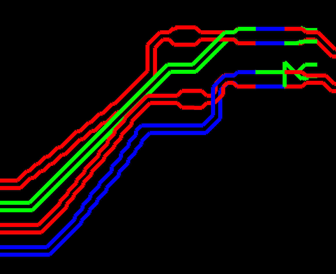
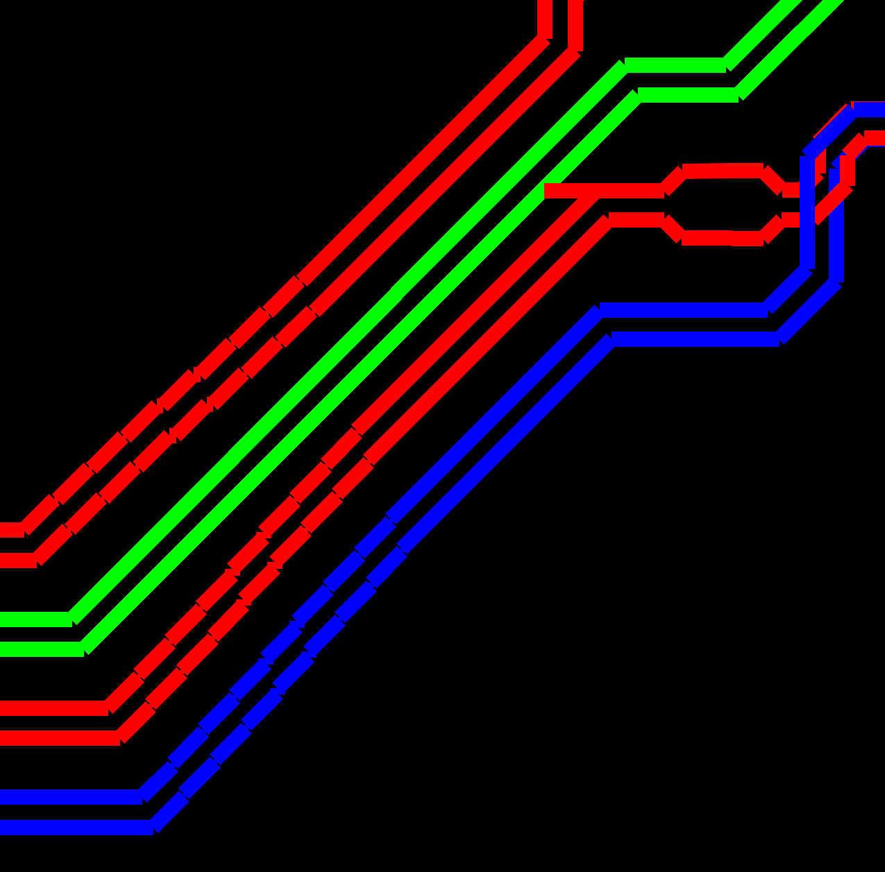
One thing I will have to be extremely careful about: ensuring that the track-to-track separation is 5mil. And as mentioned in the previous update, that's going to introduce some hair-raising issues as the separation towards the end of the tapering exercise becomes 5 mil separation. So the starting point of the tapering on the outermost tracks needs to be pushed forward by... something like.... 5 times the square root of 2 or something like that, I'll just have to experiment as I can't quite get my head round the maths until i visually see it. For example (having started the adjustments) you can see that this is getting there but each track taper doesn't start from the correct point:
Anyway anyone wishing to follow along, the source code is here: http://hands.com/~lkcl/eoma/pads
Nearly there. Once this is done I'll publish more images (and an update), ask people to take a look - there may be a bit more that needs to be done: Richard mentioned something about the TXC pair needing adjustment. Once everybody's happy we can finally send this off for pre-production sample manufacturing (if anyone would like to pay for of those do get in touch: it would help enormously as they cost USD $200 each to get made, in QTY 10). Once they're confirmed working, then at last we can set a schedule for actual production. And I can finally answer the questions that people have been asking "when's it going to be produced" with an actual concrete answer not involving "The sum of an Unknown and Unknowable amount of time plus an estimated four to five months". Hooray.