17 Jan 2014: VC0345 webcam arrived
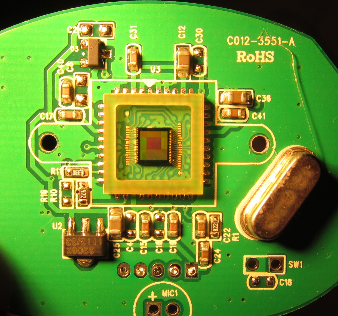
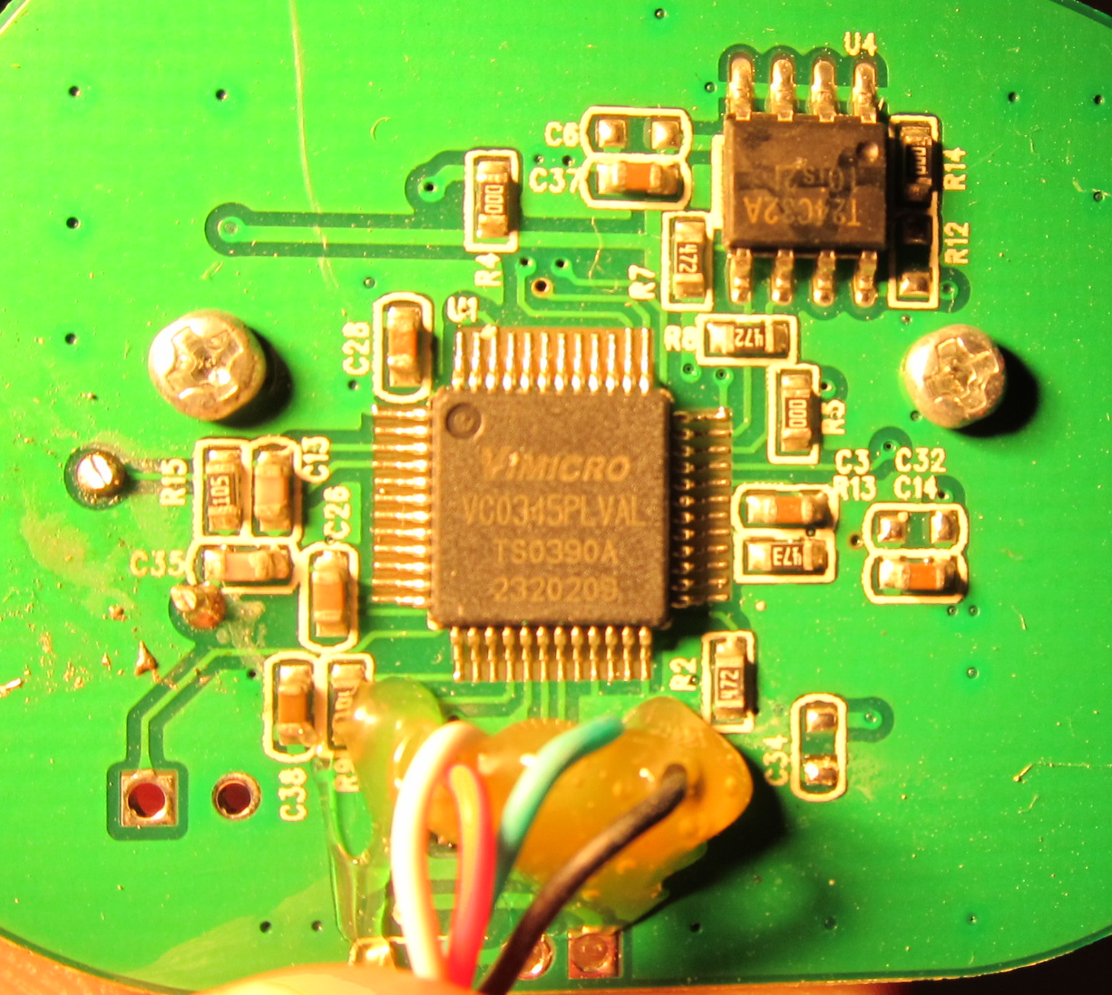
Good high-quality pictures of PCBs are hard to find: for anyone else requiring images of a VC0345 Webcam PCB, here some are. These will help confirm that the circuit used in the tablet are wired up correctly, in the absence of a response from the manufacturers, ViMicro.
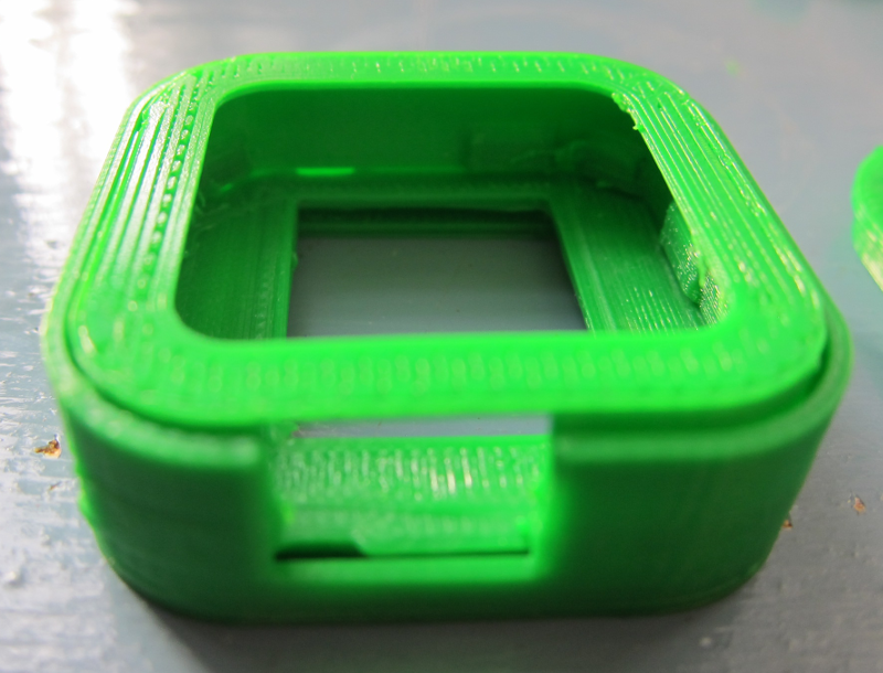
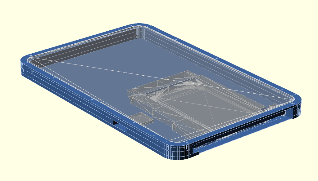
30 Dec 2014: Third revision 3D printed prototype casework
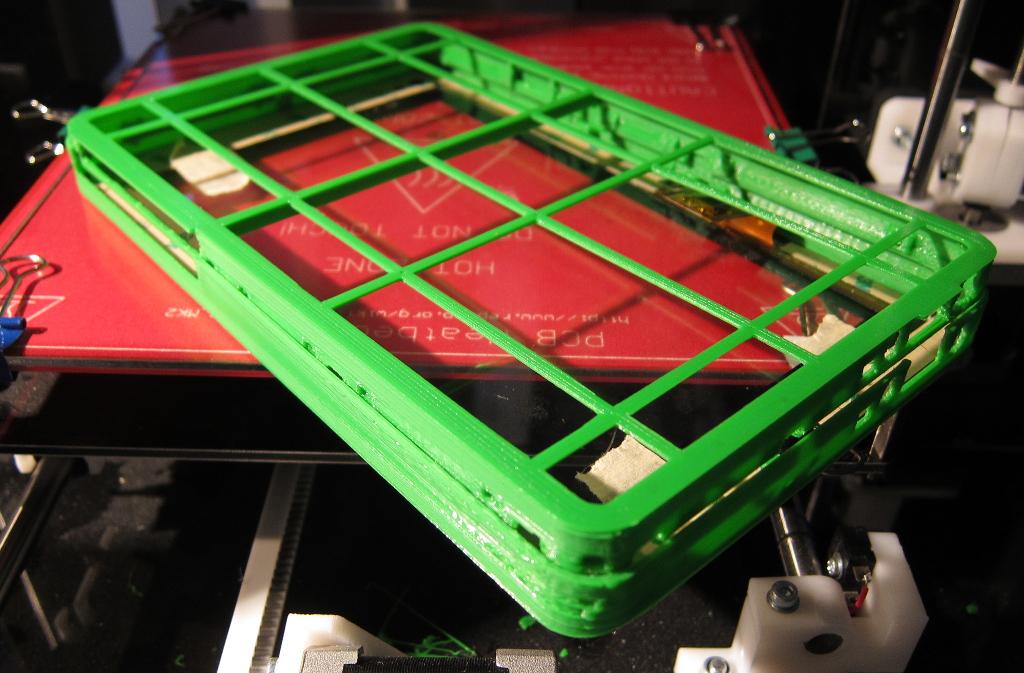
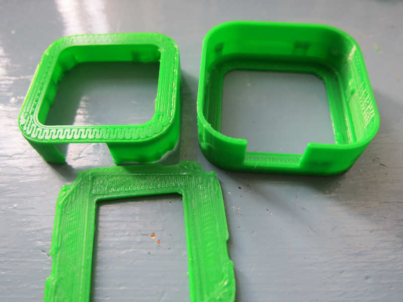
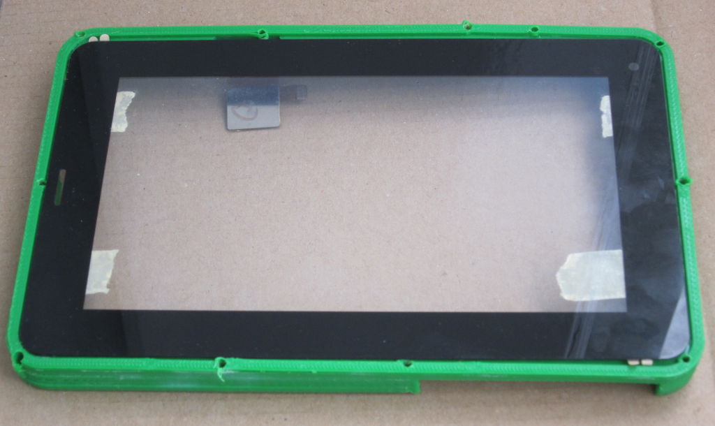
Finally a version that snaps together and does not require significant modification, only cleaning up where the printer has left trails. A better printer may produce much better results here. Shown below are the two parts that snap together (no screws required), trapping the touch panel inside. Once on, however, it does not come apart so is not being assembled until the PCB is available and confirmed working.
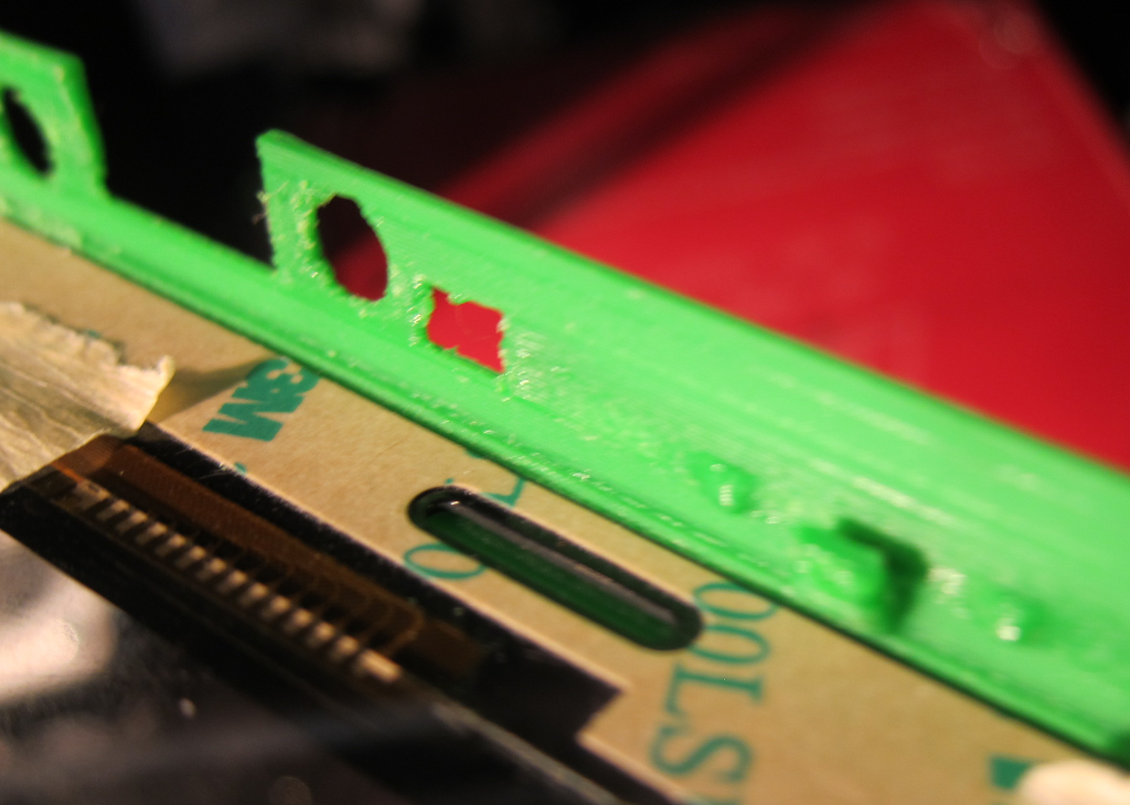
Detail below shows how the case stays together. On the inner part are indentations (usually two either side of a cut-out), and there is one indentation in each corner. On the inside of the exterior part is a clip with two bumps either side. The bumps fit into the indentations and the clips capture the inner case and ensure that it remains in contact with the exterior.
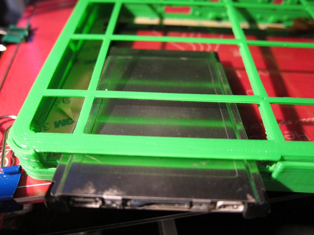
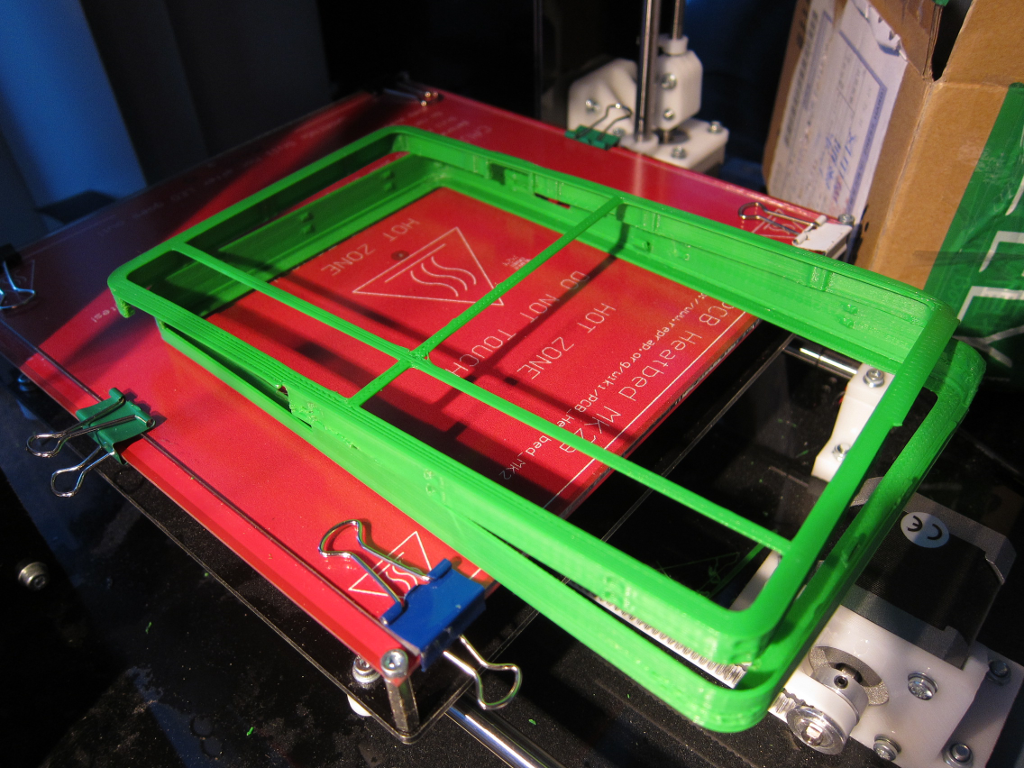
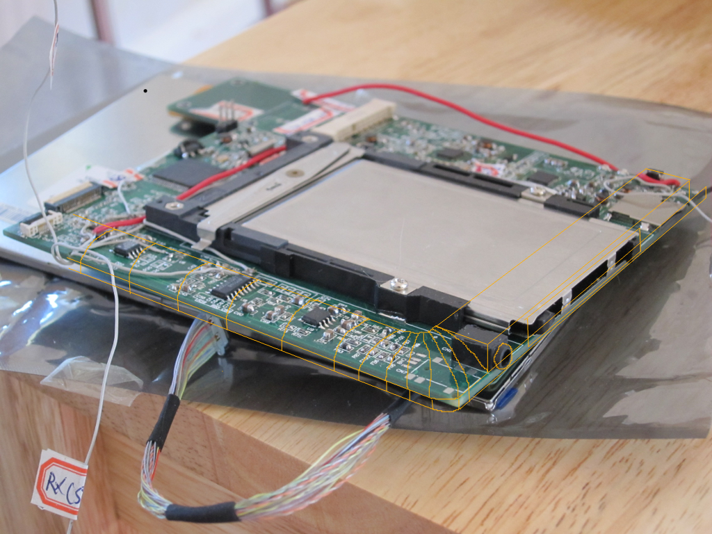
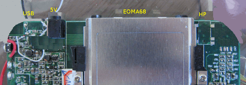
Finally it can be seen where the CPU Card goes:
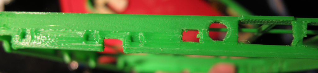
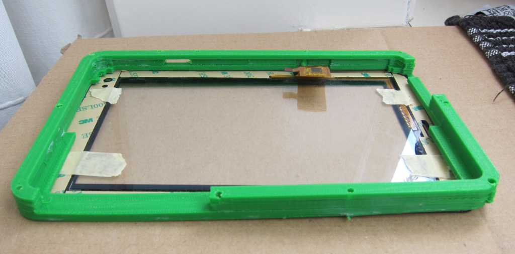
Challenges here have been that, firstly, when fitting the touch panel, the accuracy of the printer came into play, with the gcode often sending the head into the exact same corner a signifncant build-up of waste extrusion would occur right where the panel was supposed to go. Secondly, it turned out that the capture clips were in the way, preventing the panel from going into its recess at all! Two capture clips were therefore removed from near the corners on one of the longer edges. The touch panel can then be slotted into the opposite (long) edge, underneath the capture clips, then the remaining three sides bent slightly outwards at their middle points to allow the touch panel to drop in. With the plastic being so thin this is perfectly feasible. Surprisingly the touch panel provides a significant degree of rigidity to the whole assembly, although one corner may be lifted off by 5mm! In all this has been extremely lucky: the outer dimensions are around 125mm x 196mm which is just on the edge of being printable on a standard 200mm x 200mm mendel90.
25 Dec 2014: Second revision 3D printed prototype casework
After creating a first revision that could be made from laminates a more complex version that could be directly assembled as a 3D printed case was started. To save plastic a first revision 25mm by 25mm version was made:
These three parts are designed to capture the touch panel and then interlock to complete the case:
On the interior of the bottom part are small indentations that fit into recesses of the inner part. However when a larger version was attempted it was discovered that the inner part bends and doesn't catch. Some interior clips were therefore added into which the inner part slots and keeps the two halves close together. Experimentation continues - and may need self-tapping screws - as the 3D printed plastic is being kept very thin (only 2 layers the wall is turning out to be 1mm thickness)
21 Dec 2014: First 3D printed prototype casework
A 3D printed prototype of the casework has been attempted, to verify that it may be created from wood laminates. For the very first objects to be done on a new printer, it worked out well, however the surfaces are not particularly flat and had to be glued together so as to stay in position whilst being drilled. The planned holes (which would be laser-cut) are only 1.2mm diameter and a 3D printer with a 0.4mm nozzle cannot cope to make such small holes.
This first prototype however serves its purpose in verifying that the combined approach of using PDF exports from PADS, creating images from those to import into blender, then exporting STL that may be used as a ghost imported with pyopenscad to build up the actual case, is a workable albeit incredibly long-winded one. When using repsnapper to do the STL to GCode conversion and then pronterface to do the actual 3D printing it gets even longer!
Already however this prototype has proved useful in demonstrating that more modifications are needed (which affect the PCB). For example the touch panel has 3M double-sided tape that needs to stick to something, but at the top the PCB is in the way so the PCB has to be inset slightly in order to allow some edge of the case to be expanded in order for the touch panel to stick to it.
Also, in some ways it would be much better to do a full 3D printed case instead of one that is substituting for wood laminates proof-of-concept testing. The top surface of each layer is not particularly flat, having bumps and ridges, as well as not being very height accurate. This makes assembly difficult, as well as not allowing real-world verification of the design. Some more thought is required.
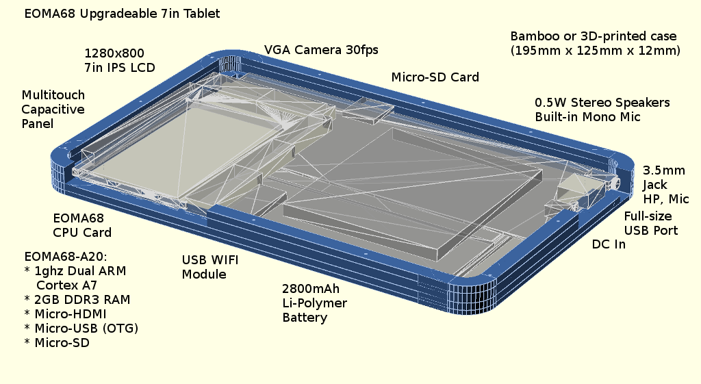
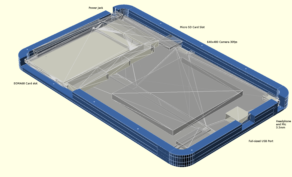
13 Dec 2014: Final Revision 3.2 CAD/CAM Layout
After noting that the LCD is deeper, the camera was found to be covered up and had to be moved to the top left corner, entirely out of the way of the LCD. This tends to be the primary reason why cameras are in the top corner of tablets: the layout in other locations is almost impossible. With that as another inviolate requirement, the rest of the layout falls into place and is now considered final.
Top left is the VGA camera. Along the top edge is the tablet's MicroSD card slot. Along the right edge from top to bottom is the 3.5mm Headphone Jack (including stereo headphones and microphone), followed by a full-sized USB Host port, then the power/reset button and then the DC power jack. The CPU Card slots into the bottom left corner along the front edge, as this allows the battery to take up the majority of the right-hand side whilst leaving the LCD's taped-down LVDS Converter PCB completely clear.
Battery-wise EEMB have a standard-sized battery at 68.5mm x 89mm x 5.3mm which works out to a 2800mAh capacity. There is however space for larger batteries (up to approximately 85mm x 100mm x 6.3mm) which would give more than a 50% increase in capacity to around 4500mAh, however it would require a custom order from EEMB which has a MOQ requirement so is not being immediately considered.
Casework-wise, the layers stack up to between 12mm and 14mm depending on the chosen thickness and material of the top and bottom layers. Wooden laminates throughout would require a 14mm thickness, whereas if stainless steel is chosen for the base then a 12.1mm thickness would be feasible, as long as a cover arrangement could be made to ensure that the sharp edge of the stainless steel is not exposed. Possible solutions there involve filling in the holes with acrylic, which, around the Power, USB and Headphone sockets is likely to be needed anyway as the power and charging LEDs shine through from just behind the power button. It's rough, it's 3D printable, the parts can be 3D printer be laser-cut from any material and stacked without gluing, and it's workable, so we go with it.
12 Dec 2014: Revision 3.2 CAD/CAM using Blender and OpenSCAD
After nearly finishing the revision 3.1 PCB layout, a screenshot was overlaid onto the Blender CAD/CAM and found to be completely wrong. The layout therefore had to be redone (again), with the lesson learned to include the casework layout as part of the iterative process.
The actual original development of the blender file took weeks, however now that all the parts exist actual modifications are relatively quick and simple, meaning that iterations between three separate programs (PADS, Blender and OpenSCAD using pyopenscad) is not a huge challenge once underway. The first screenshot below shows how two (opaqued) images help ensure that 3D blender blocks are placed in suitable locations. There are two images: the first is (another) screenshot of the PADS PCB components, whilst the other is a picture of the touch panel. Both images are set to near-transparent levels so that the lines (bright red) of the blender-rendered components can be created and adjusted to fit the PCB images. For example: along the top edge it can be seen that the film connector from the touch panel is arranged to line up with the 10-way connector of the PCB.
After exporting to an STL file, which may be imported with pyopenscad, a second screenshot shows how the casework can be fitted around the internal components. As the layout of the casework is done in python, adjustments are incredibly easy to iterate, and are much easier than using GUI tools (such as Blender). The problem with using a mouse is that it is not only inaccurate but also there is often absolutely no control over linking even two numbers together so as to avoid either mistakes or extra work. By specifying numbers as variables in python it is possible to simply substitute those into functions. Simple, straightforward, accurate, efficient and effective, and with key re-mapped bindings used in vim to not only save the file but also to run the python interpreter to re-generate the OpenSCAD file (where OpenSCAD is set to automatically recompile) iterations are fast, as well. The vim key binding is as follows: :map , <Esc>:w<CR>:!python car_model.py<CR><CR>
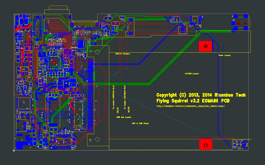
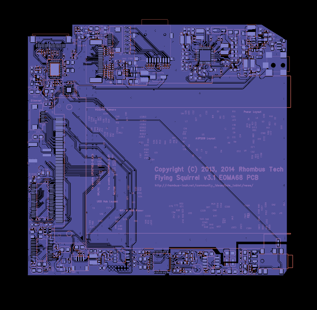
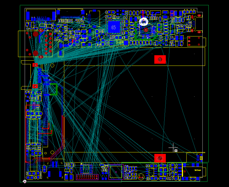
10 Dec 2014: Revision 3.2 PCB
A decision was taken to redo the entire PCB layout, after discovering the Hannstar 7in 1280x800 LCD and a 10in 1280x800 from the same manufacturer. A total redesign is required for two reasons. Firstly: the LCDs have completely different pinouts. Secondly - more importantly - the LG 7in display had a PCB 2mm high on the left-hand side but the Hannstar 7in LCD has its LVDS conversion PCB at the bottom. In order to ensure that the thickness of the entire tablet is not increased by the height of the LCD's on-board conversion PCB, it is necessary to completely redo the layout, to a 5.5in x 3.2in PCB.
So a decision was taken to make this PCB be useable for a 10in netbook as well as a 10in tablet and a 7in tablet. In order to ensure that the connectors all fit on the left or right edges only, the Headphones, USB and Ethernet have been moved to a separate (small) PCB that will be reached via a 40 pin dual-row 0.4mm pitch B2B connector (top left corner). The Camera IC and Touchpanel connectors have been left in exactly the same relative positions, but this is literally a complete re-layout that is still in progress.
Moving the USB, Headphones and Ethernet to a separate PCB is very handy, as different connectors for a particular purpose may be chosen. For example, as this is quite a thick tablet it is perfectly reasonable to put a full sized USB (A) connector on it, rather than the smaller Mini or Micro USB. Also, for repair purposes, replacing one small PCB is much cheaper than replacing the entire unit, so for that reason moving the DC jack to the smaller PCB is under consideration as well. As there is an on-board AXP209, still, battery charging may take place as well via a USB-OTG socket on a CPU Card (if there is one).
4 Dec 2014: First revision PyOpenSCAD prototype casework
Using pyopenscad a first revision of the tablet casework has been drawn up. The border surrounding the touch panel is 5.0mm, and it is made up of layers (1.5mm, 3.0mm, 4.0mm, 2.5mm and 0.2mm) so that, except for the 0.2mm base which should be of stainless steel, construction may be made either of wood laminates or of 3D printed parts. The first layer is a surround around the touch panel. The second is inset from that, and the touchpanel is supplied from the factory with 3M double-sided tape so may be stuck directly to the second layer. All layers would be attached with ten 1.5mm diameter screws or bolts. Total thickness comes in at 11.2mm.
From the picture below it can be seen that the MicroSD slot is inset, as is the headphone and power jack. The Power button will need an acrylic inset as there are two LEDs just behind the power button.
Straight-backed sides have been deliberately chosen both for ease of hand-assembly from 3D printed or wooden laminate parts, but also so as to give a much more simple and solid feel. Also this gives about 10% extra battery space (the present battery chosen was based on curved sides).
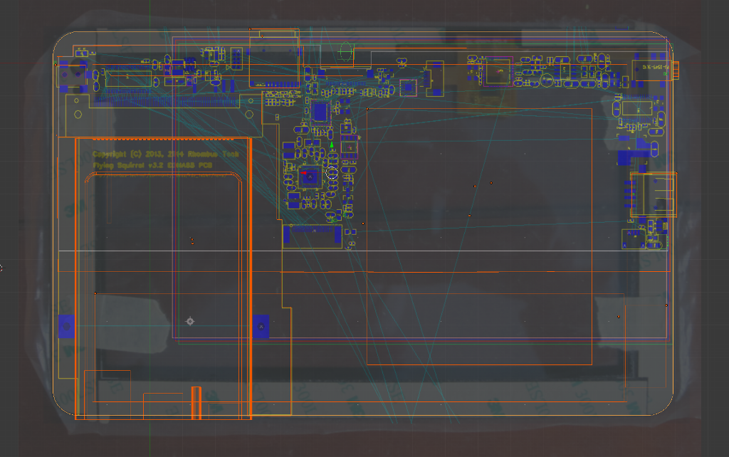
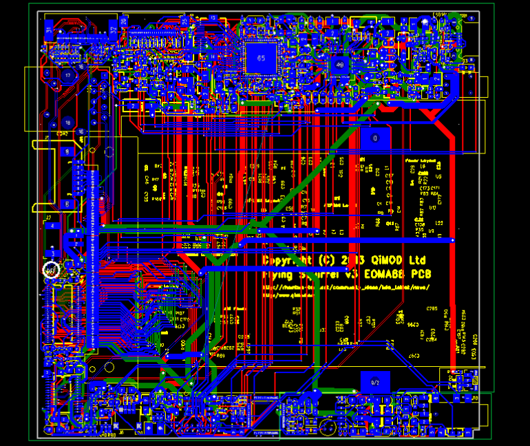
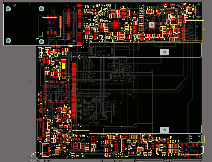
3 Dec 2014: Revision 3.1 PCB
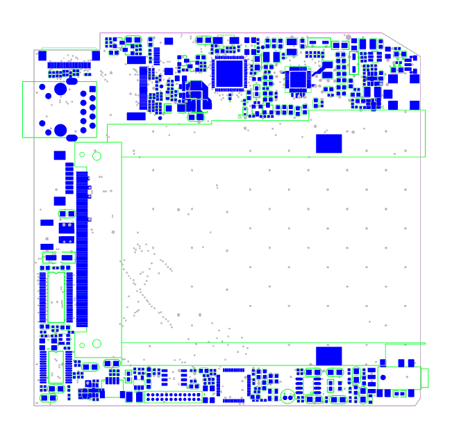
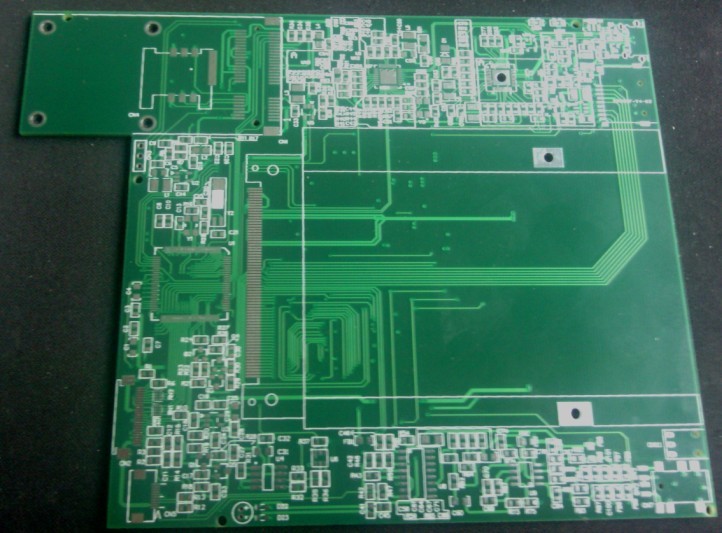
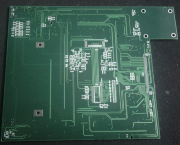
After the Revision 2.1 EOMA68-A20 prototypes were successful and the Micro-Desktop as well it was time to return to the Tablet PCB. A Micro-SD Card slot has been added as a direct connection to the EOMA68 interface. Significant layout improvements have been made over the Revision 3.0 PCB layout, including the discovery that the Texas Instruments SN75LVDS83B could be turned around 180 degrees and the pinouts with the RGB/TTL interface of EOMA68 lined up perfectly! Also by accident a pin-compatible china sourced LVDS IC has been found. The image below shows the component layout and the top layer. All components are still top-side: there is hardly any free space anywhere on the board, with the CPU Card and the Amphenol PCMCIA connector taking up the centre. Several corrections were made to the Silkscreen: it had not been previously noticed that there were overlaps onto component SMT pads! Iteratively printing out the gerber files and examining them with an external tool clearly showed where the errors were in ways that are not intuitively obvious to replicate from PADS 9.3
14 Dec 2013: Third revision CAD/CAM Casework
Work on the case has started (from scratch) due to the former designers
requiring an enormous "release" fee for access to CAD/CAM files,
which had not been part of the negotiations. In some ways this is good
because they weren't listening to what was required, and made a large
number of mistakes. What is good about what they did however is that
a) they provided a physical prototype that could be "cut to shape" and
b) the prototype illustrated what was
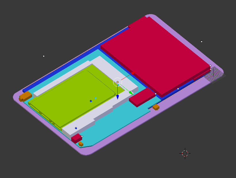
In this case work is progressing by creating CAD/CAM models of all the parts, using blender. This will help ensure that the casework will fit around the parts. In white is the Amphenol PCMCIA holder; green is the EOMA68 CPU Card. Cyan is the Flying Squirrel PCB. Dark blue is the LCD. Light purple is the touchpanel. Various other blobs represent battery, WIFI module, headphone, power, Camera and reset switch. With all these parts in place it is now possible to create a case around them. With access to the actual CAD/CAM model it is also possible, prior to physical creation of a prototype, to spin the whole thing round and check from all angles.
10 Nov 2013: Third revision finalised
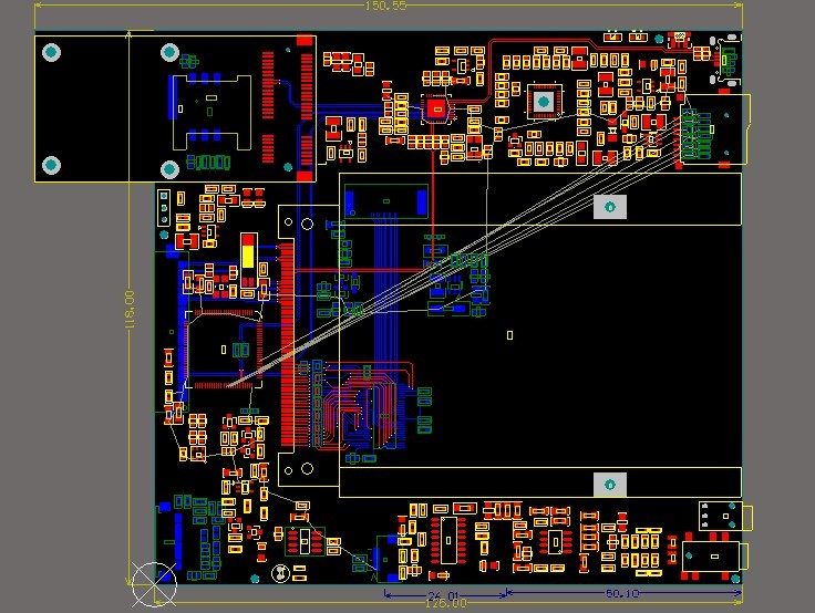
The revision 3 gerbers have gone to the factory to be analysed. If they pass inspection then some sample PCBs will be made up and populated. For what appears to be such a simple task - "make a tablet PCB" - this is an amazing amount of fuss, and very little spare space! The PCB is around 10cm square yet there is no room for additional components.
Partly this is down to it being entirely single-sided, partly due to optional capabilities for alternative purposes. The reason for the board being single sided is not so much to reduce cost (which will be an interesting side-effect) but because the 6mm PCMCIA socket is already too much for an extra 2mm clearance of double-sided components to be acceptable. When in a case the product will come out at just under 13mm. 6 for the PCMCIA socket, 1.2 for the PCB, 3mm for the LCD, 1.5 for the touch screen glass and 1mm for the plastic casework. Alternative materials such as magnesium alloy have been considered, in order to get the thickness down. Still, the critical part is the PCB: let's see how that works out.
1 Nov 2013: Third revision routing
With some help and guidance from a lot of people, on design rules and PCB layout, the routing is progressing. The auto-router simply doesn't cut it on the differential pairs, so these have been initially laid out by hand, then allowed to be resized (length-wise). Likewise after several false starts a decision was taken to route the RGB/TTL by hand as well. Although the auto-router could make the connections with some hints, it just looked dreadful.
Also the PCB Factory have been very helpful, asking the right kinds of questions that lead to exploration of "impedance" for example. So many details to deal with! Many thanks to Ryan for the hints about only allowing 90-degree entry into square pads: this has got rid of more design flaws than anything else.
The QFN and the LCD connector pad sizes are tiny. The AXP209's clearance is only 5.8mil. Also, it's incredibly densely packed. So, surprisingly, even though this is "only" an I/O Board, minimum track width has had to be cut to 6mil, and track-to-track of 5.5mil has had to be allowed.
Also a nice addition: it turns out that the 1024x768 LP097X02-SLA3 LCD is not a million miles different from the LD070WS01 in terms of connections. Several (20!) 0R resistors have just about fit under the connector, making it possible to try a 9in 1024x768 LCD out on this board.
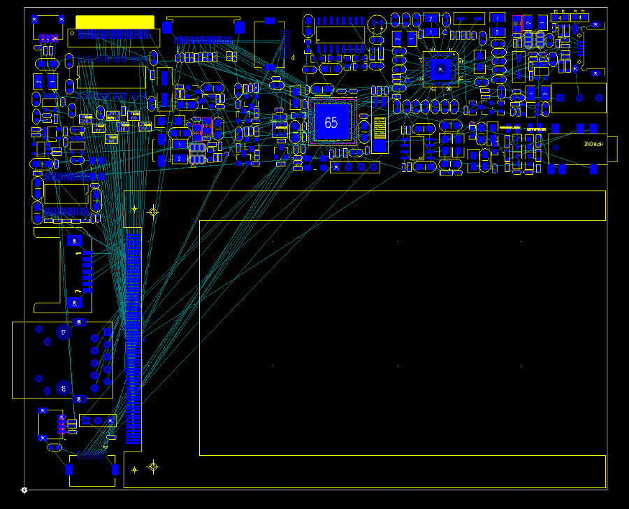
28 Oct 2013: Third revision component placement
Some very fast development over the past 4 days gives a preliminary placement for components, showing that this is actually achievable and that everything is going to fit. Connectors and components from top left downwards are LVDS/LCD, Ethernet, SATA, 2-Axis sensor, 3.3V WIFI, SN75LVDS83b, FE1.1 USB Hub, Battery, I2C EEPROM, 20-pin expansion header, USB Audio IC, Microphone, TDA2822 speaker driver, Headphone socket, Power switch, EOMA68 CPU Card socket, DC Power Jack, Micro-USB, 2 LEDs, AXP209, ATSAM4S, Touch panel, Camera and finally back to LVDS LCD connector. It's a pretty dense board, almost 105mm square, with virtually no room to spare. The middle is deceptive: no components can go where the EOMA68 CPU Card is, and there can be no underside components either, in order to get the thickness down.
The nice thing about shrinking the board size (it was originally around 125mm x 117mm) is that the battery size can now increase, and the styling can be more curved rather than rounded.
24 Oct 2013: Third revision begins
After some rapid evaluation and decision-making the third revision begins with a completely different Embedded Controller: an ATMEL SAM4S. The reason is simple: the SAM4S has USB2 and support for Digital CMOS Cameras via a suitable high-speed parallel port. The STM32F103 could not handle the camera data, and the STM32F207 was far too expensive.
The decision was taken to also use a QFN64 version of the SAM4S, and to reduce components down one size: 0603 becomes 0402, 0805 becomes 0604. This has meant that there is enough space not only to fit all components on TOP but also to add space for optional full-sized Gigabit Ethernet jack, SATA connector and a second FPC-12 with a small set of expansion pins coming from the SAM4S, mostly containing SPI pins with three Chip-select lines, as well as one PWM and one ADC.
The DACs will still be used with a TDA2822D, and one ADC will still be used with an LM13700M. A prototype circuit is going to need to be built to use the 2nd channel of the LM13700M as a unity gain amp in order to use it for impedance matching with the 1st channel. Normally a high-gain op-amp would be used for this purpose, but if that is done here then the cost of the three components (TDA2822D, Op-Amp and LM13700M) exceed the cost of using a dedicated I2S CODEC. This may end up being done anyway because it would get better quality sound (although this is hard to detect on 0.5 watt speakers!)
Here's progress so far. The components have been laid out and it would appear that everything fits. Whether this is feasible with a 4-layer PCB is another matter!
12 Oct 2013: 2nd revision, Camera Status Report
Status update at the PCB page). After spotting and correcting mistakes in the camera sensor power-up circuit, attempts to provide a valid clock via MCO proved frustrating but ultimately successful. It was then possible to examine linux kernel device driver sources and replicate the I2C commands needed to set the camera sensor up.
However... closer examination of adamgreig's "followingrobot" code shows up some problems. Firstly, Adam set the sparkfun-supplied part to a 6mhz clock rate. Attempts to set a 6mhz clock rate on the GC0309 $3 part were not successful (12mhz however was). At 12mhz, the pixel clock rate is also going to be 12mhz. At 72mhz this leaves only six instructions in which to read the camera data on an extremely tight CPU-intensive loop which must not be interrupted, even if audio data is to be serviced.
Others who have used a chain of External GPIO - EINT - Timer - DMA - Port Read have found that this maxes out at 6mhz for an STM32F103, which is not enough. Basically we're going to have to go for an STM32F207VCT6.
The STM32F207VCT6 is a 120mhz part instead of 72mhz, it has full 480mb/sec USB-OTG instead of 11mb/sec USB Client, it has 4-bit SD/MMC, as well as I2S (which can be used to connect a high-quality MAXIM or Wolfson Micro Audio IC), and, most importantly, it has DCMI. The combination of 48mhz 14-bit DCMI plus 480mb/sec USB2 Audio would mean that it would theoretically be possible to do a camera on the Flying Squirrel with a 1280x720 resolution @ 25fps! A mere 640x480 @ 30fps would not even push things hard.
Luckily, the STM32F207VCT6 is pin-compatible with the 103 equivalent, and the Revision 2 schematics have already planned ahead for the possible upgrade. Connecting the camera sensor to the DCMI interface is a simple matter of changing which pins are used: there are no extra circuits required. So - bad news that turns out to be good news, with no real significant schematics changes, reduced development risk and a better product anyway. All for what is likely to turn out to be about another $0.60 on the BOM.
08 Oct 2013: 2nd revision, DAC Audio prototype PCB: success
Status update at the PCB page). After considerable experimentation a decision was made not to use PWM for the audio output, and to use the two 12-bit DACs instead. The primary reason was concern over how the TDA2822D (which is a 0.5W Class B amplifier) would react to high frequency edges of PWM output.
So instead, after finding an STM32 application note which outlined how simple it is to use an STM32F to read from an SD Card and play back WAV files using DMA, a decision to try that out was made. The first experiment showed huge clipping: the DACs output 3.3V peak-to-peak. Ramping the DAC output back to 1/25th of its dynamic range fixed that, and gave a sine wave on the output. Further experimentation with a resistor bridge (200k - 2.4k) gained back the full 12-bit dynamic range of the DAC.
As the TDA2822D is a 0.5 Watt amplifier, and the speakers are 8mm x 18mm the volume is not exactly spectacularly loud, especially at low frequencies. A larger capacitor (470uF instead of 100uF) will help slightly at the low end, however for voice this solution is perfectly adequate, and there will also be a headphone option. Video demonstrating the circuit and explaining the software is here:
05 Oct 2013: 2nd revision, ADC (for Microphone) confirmed operational
Status update at the PCB page). The firmware for the Flying Squirrel is making good experimental progress. An interesting learning curve with the ADC has shown that it's necessary to carry out a hard reset of the STM32F ADC subsystem: it's insufficient to just power it off and on again, it's necessary to power off, reset, then configure and finally switch on. Once this was discovered (through random internet searches) reading the ADC was very straightforward, and also successful.
The next part was making it easy to read the ADC values, for debugging purposes. This was achieved by turning the STM32F USB gadget into a CDC ACM (USB Serial) interface. Copying one of the libopencm3 examples turned out to be very straightforward. Next up will be adding a Timer around the ADC as well as using DMA. Enough code exists: it just needs to be successfully plugged together.
The actual circuit around the LM13700 however is a different matter. The layout from March bears absolutely no relation to the example schematics in the datasheet! Fortunately, there are three LM13700 ICs now available to experiment with, as a means to create a working amplifier circuit.
Software-wise the microphone is turning out to be straightforward as expected, and the progress being made will help accelerate the development of the tougher task - the camera. The camera will require not just DMA but possibly some very tight post-processing and more. The fact that it's now possible to interact with the STM32F as a USB-Serial device will make debugging that much easier.
Update 17:00hrs - a video showing the progress made.
03 Oct 2013: 2nd revision, more hardware confirmed working
Status update at the PCB page). The 3-axis sensor has been confirmed as being a 2-axis MXC6225 sensor, and, through a small python program that opens the /dev/mxc622x entry and carries out a couple of ioctls, confirmed as working. Also the address of the I2C EEPROM has been confirmed (and the elinux.org EOMA68 specification updated accordingly). The reason for updating the specification is because the mistake was made in reading the AT24C64 datasheet: there is no point having a specification where the EEPROM's I2C address is impossible to match, with an address where there are simply no EEPROMs available on the market.
For USB, a mistake has been discovered in the schematics: there is a 1.5k pull-up resistor missing from the USBDP line. Currently there is a resistor precariously perched on top of the STM32F, wired between a USB cable that's soldered directly to the STM32F pins. The libopencm3 usbhid example was then uploaded, and the STM32F responded by turning into a mouse.
Next up was apalmer's audio patches to libopencm3, along with some gratefully-received demo code. libopencm3 as it stands does not have ISOCHRONOUS usb, nor proper support for USB attributes and descriptors: apalmer's patch adds this capability (USB IN only). The code was compiled and demonstrated as successfully working, by being able to record an (accidentally) reversed sine-wave which was generated by DMA reads off of the STM32F.
All in all this is extremely good progress. The challenging parts are going to be the speakers, microphone and the camera. The microphone should be reasonably straightforward: read the ADC and output it as data. Speakers: last time they were tried, the amplifier IC was overloaded - some care has to be taken here. The camera is quite involved: it needs to be powered up carefully (by programming the AXP209 to output 2.8V), then the Camera can be programmed over I2C. After that the Master Clock can be enabled at around 15mhz, and then data read back in a very fast interrupt handler and stored for transfer over USB. This is where it will get... interesting...
29 Sep 2013: 2nd revision, status update with EOMA68-A20 CPU Card
Good progress on the Flying Squirrel Tablet (currently being maintained at the PCB page). Some short-circuits were found between pins on the PCMCIA header, between the I2C lines and the RGB/TTL. The pins had to be dug up (legs now kicking in the air) and wires run over to appropriate points on the PCB instead. Now that's done, all of the I2C devices (AXP209, Touchpanel, 3D sensor, I2C EEPROM) are all detectable, and the LVDS Driver IC is activated again and the LCD operational.
Also it's been discovered that Wits-Tech shorted out VBUS to ACIN without informing us. This means that when a USB-OTG cable powers up the CPU Card at the same time as 5V power being provided that the two fight for dominance of the 5V rail. The AXP209 on the I/O board freaks out and shuts down. To "fix" this - i.e. be able to carry on working - the 5.0V line has been cut out of a MicroUSB cable. A proper fix will involve either reworking the CPU Card or putting in power-detection on the I/O PCB.
27 May 2013: 2nd revision decisions
A review of the 1st PCB along with a first attempt at casework design highlighted some gotchas. One of the requirements is to have nicely rounded corners, similar to the GPL-violating CT-PC89e which kicked off this entire project. Note how the connectors are inset (like a dormer roof):
This is what we really want. The problem is highlighted by the following picture. Look closely at the wire-frame, and note that the Headphone socket isn't yet installed:
For this to happen, the connectors need to be moved inwards, which means that one of them has to go. As it'll be over USB 1.1 (via the STM32F), that means that the best candidate to go is the Micro-SD. Given that there is already a Micro-SD slot on the EOMA-68 CPU Card, this is not a great loss.
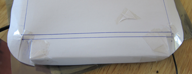
We're having a little difficulty explaining the concept to the design house so have come up with some prototype mock-ups (made out of thick paper). Rather unfortunate, but we feel it is better to get such a significant design error corrected than to try to sell something that would look utterly pants. With curves at the corners, the tablet looks the part. Not like a brick, but like a decent machine that's easy to hold as well.
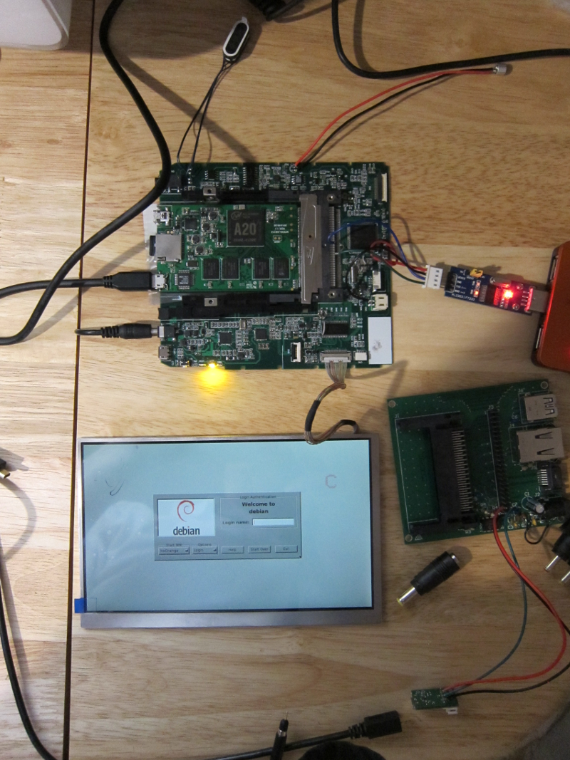
11 Sep 2013: 2nd revision, working LCD with EOMA68-A20 CPU Card
Thanks to Joe (of GPL-squared) for helping to spot some schematics errors swapping the LCD-HSYNC and VSYNC in one area and LCD-DE with HSYNC in yet another: removing one of the bank of 4 resistors and replacing it with 0.5mm wires in a tiny tangled cross-over mess allowed the picture below to be taken, which demonstrates several things:
- Firstly, that the EOMA68-A20 has a working RGB/TTL LCD interface (at least up to 1024x600).
- Secondly, that the Flying Squirrel's LCD power and Backlight circuits work (and everything else driving it, including the 2nd AXP209 PMIC as well as the 3.3v regulators)
- Thirdly, that the PCMCIA connectors appear to have been massively over-engineered (they were spec'd for only 33mhz 16-bit PCI data!) which is good news because the RGB/TTL lines are being driven at about 78mhz for this LCD, alone.
- Fourthly, that the STM32F can and has been successfully programmed to bring up 3 GPIO lines, controlling LCD power, Backlight Power and LCD PWM brightness (currently set as a plain GPIO at 100%).
So that is quite a lot that's properly working. In combination with the testing carried out by several people on the arm-netbooks mailing list, which has confirmed that both Ethernet and SATA are functional, this successful test confirms all the major high-speed functions of the first CPU Card in the EOMA68 series: the EOMA68-A20.
The next stage will be to bring up the Touch Panel (I2C Bus), check the accelerometer (I2C bus again) - these should be fairly easy. After that it's into some libopencm3 programming, to create a PWM-based Stereo Output driver that will register as an AC97 USB audio device. Microphone (14-bit ADC) will follow on from that, and last but not least will be to port adamgreig's "followingrobot" CSI camera code from ST's libraries over to libopencm3.
Lots still to do but a working 1024x600 IPS LCD is a major step forward.
8 Apr 2013: First PCB back from the factory
Woo! After the China spring break, the PCB for the Flying Squirrel has arrived back from the factory. It's yet to be populated with components (which is to be done by hand) - more news when it happens.
31 Mar 2013: Follow-up images from the designer
Here is a follow-up from the designers, showing progress so far. Samples for the Micro-USB, Micro-SD and SIM Card arrived; the Micro-USB was compatible but the Micro-SD was deemed to be inconvenient, both for manual soldering as well as for later mass-production. The SIM Card turned out to not have a locking mechanism (hard to tell from the datasheet). So a decision has been made to leave 3G until the next revision, leaving the Mini-PCIe slot as intended by the client: for USB-based WIFI modules only.
Overall the specification of this tablet will be on the high end for connectivity: dual USB ports and dual Micro-SD cards, because the EOMA-68 CPU Cards will typically have one USB and one Micro-SD.
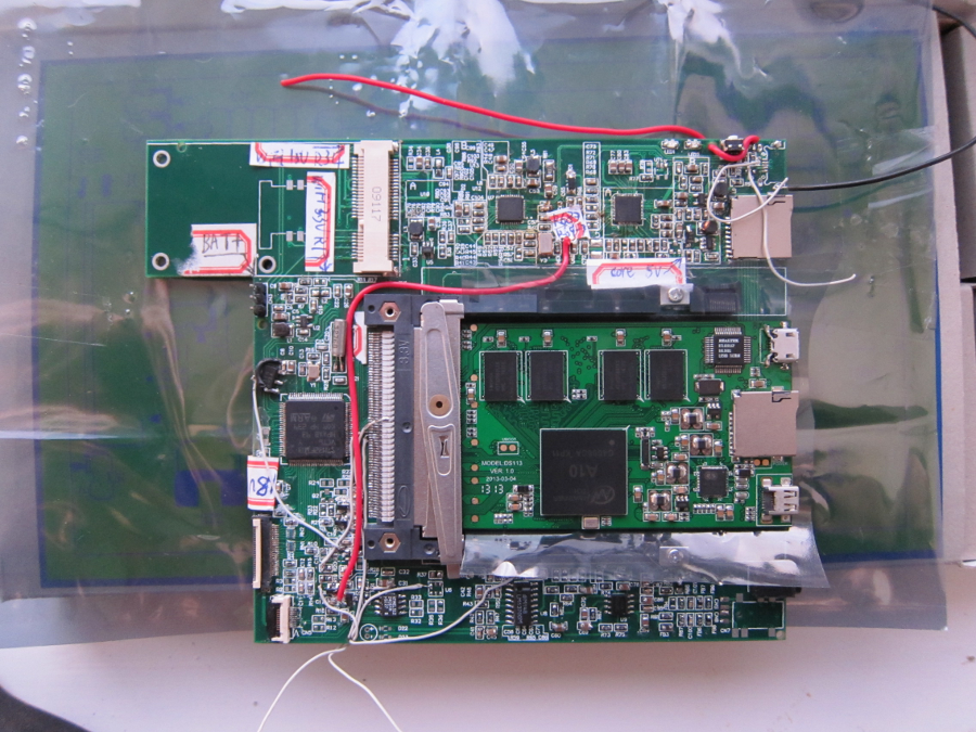
15 May 2013: Populated 1st Revision PCB arrives
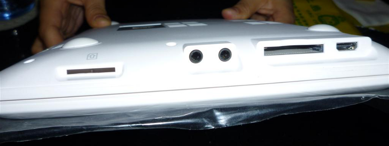
The 1st Revision PCB has arrived, strewn with wires in preparation for the 2nd revision. Component placement is 99.5% good: there are some parts on the underside that are over 1.5mm height clearance, and the LCD will be at the back. Along the right-hand edge in order from top to bottom is Micro-USB OTG, Micro-SD, then on the A10/20 EOMA-68 CPU Card is a 2nd Micro-USB OTG, a 2nd Micro-SD, Micro-HDMI, then back onto the PCB is 5V Power and Stereo Headphones and Microphone. In addition to an on-board programmable embedded controller and a user-replaceable USB-based MiniPCIe WIFI slot, all in all it makes for a pretty awesome tablet.
The next phase is, whilst the casework is being done, to get the software up and running for the STM32F. Backlight, Touchpanel, I2C devices and bring-up of the STM32F have all already been done because they are wired directly to the EOMA-68 interface. However, the audio (speakers and mic) are being done in software as PCM (including volume for the microphone) and the Camera will require the use of the "followingrobot" project source code. Fun ahead: a kernel driver is needed as well!
8 Jan 2013: 1st attempt at a PCB layout
As a first approximation, this is an inexperienced attempt to create a layout for the Flying Squirrel. Quite a lot of difficulty has been experienced convincing Chinese ODMs to stop trying to 'recommend Android, A10, A13, "we can do it this way much better, you don't wanna do that Old-School stuff", where's the HDMI interface, surely this isn't an actual tablet, it's got no processor, what's it doing with LVDS, did you actually want a screen, it must be some sort of voodoo magic industrial device, therefore we must charge you more money'. Eventually a decent industrial-style designer was found who wasn't fazed by the sheer oddness of putting in an STM32F, and who really liked the EOMA-68 concept. I like Franson.
The size of this very very early PCB layout is 120mm x 175mm. The size being aimed for is around 117mm x 160mm. Also, the PCB is being designed so that as a Tablet, all connectors are on the right-hand edge (another USB-OTG, another Micro-SD, Headphones and Power), and, also, for future products and also for engineering purposes, an extra USB2, an Ethernet RJ45 and an eSATA can be added. Bottom left is a temporary component (that happens to have 54 pins), which will be replaced with a PCB decal for a JAE Mini PCIe socket shortly.
15 Jan 2013: 2nd attempt at a PCB layout
The "no idea how to do this, maybe it will save time and costs and it's fun anyway" PCB layout is progressing well: it's now down to 125 x 113mm (5 x 4.5in) and contains approximations of the various components (PCB Decals) which a professional PCB designer should at least be able to run with. Experimentation with the Auto-router has been fun and games: it's not perfect, but laying out some parts by hand (including the VCC-3V3 and VCC-5V0 lines), the RGB/TTL portions and the AXP209 fan-out has got round most of its weaknesses.
Component positioning has been an interesting part of the experimentation. Top-left is the USB-based Mini PCIe, with a Litkconn SIM Card holder underneath. The FE 1.1 USB Hub fits top-centre. The AXP209 and the majority of the power conversion circuits fit top left, and the Micro-USB and Micro-SD fit in the very top left corner. The 100-pin STM32F is in the middle of the left side: it's a tight fit. The 5V Power In connector hasn't been done yet: it's in the bottom-right corner and a large 3-pin SIP connector has been chosen as a temporary substitute. Next to that is the Audio jack: speaker headers just to its left. In the far bottom left corner is the Microphone. To the right of that is the CSI Camera Interface; to the right of that is the LVDS connector for the 1024x600 IPS LCD Panel.
To the immediate right of the STM32F, a 60-pin expansion header was chosen as it saves a great deal of space: this connector will allow the exact same PCB to be used in a larger device including a low-power laptop. The pin-outs include 20 STM32F pins (for use as a keyboard matrix), Ethernet and SATA. Potentially there is room to route the GPIO pins from the AXP209 as well, just... because they're there.
The actual layout has been quite straightforward: using "grouping" has allowed the components to be moved about conveniently, as well as allowing their Net lists to be selected and specific track widths applied. The majority of components, despite the small size, have been kept on TOP in order to ensure that there is good clearance for the LCD Panel. Potentially, with a small increase in length in order to accomodate the Expansion Header, all components could actually be moved to TOP, thus reducing the manufacturing costs. The kicker will be the LVDS Panel, as a cable would be needed which folds back and reaches the other side.
10 Nov 2012: Headphone and Mic Circuit
This needs review: there are just enough pins to connect the headphones up to the STM32F using the two DACs and two PWMs for volume control: this is in addition to the PWM-controlled speaker outputs, giving two separate stereo audio channels. Help is needed in wiring up the mic suitably, as well as connecting the headphones to the LM13700.
12 Nov 2012: Headphone and Speaker Circuit
This variant on a headphone and speaker circuit is much simpler, and requires less pins on the STM32F. The headphone socket is used to switch off the two speakers. An ST LM2822D was found (and then a very low-cost China equivalent). The LM2822D is however only 380mW per output, which is a little on the low side. Potentially two of them could be used in Bridge mode, giving 0.8W per channel. The main benefit was finding a suitable PWM filter circuit which could be connected to this amplifier: there was some concern over the Class D MOSFET H-bridge approach creating too much R.F. even though it is much more efficient than Class AB. The H-bridge also required four pins, and could not be connected to the headphones, requiring a separate circuit. This approach is much simpler.
22 Mar 2013: Proper attempt at a PCB layout
Many thanks to Franson of Quick Embed, they are redoing the tablet layout. Many of the decisions and requirements were not documented prior to the hand-over, so it has been necessary to point a few things out along the way. Franson's team however are absolutely great, recommending parts that are easier to obtain than those originally sourced (or thought to be a good idea at the time).
The one bug-bear however is the touch panel. The customer requirements were for a camera to be on the long side (a la Kindle Fire). The reason is simple: any two people making a two-way Video call will, unless the camera is close to the centre of the screen, look like they are incapable of focussing on the person in front of them. Unfortunately, the low-cost $7 touch screen mold that's Public Domain and uncopyrighted (touch-screen designs are copyrighted! in China! insane irony....) and available easily in large volumes has a camera hole in the corner. Costs being what they are, it will be necessary to push this back to the 2nd revision.
Here's progress so far by the PCB designer from Quick Embed. It's pretty close to the version done earlier, except that parts are the right size, and actually available.
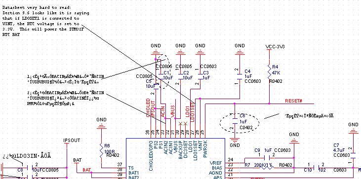
10 Nov 2012: AXP209 Real Time Clock Power Out
The AXP209 is an awesome Power Management IC - the only problem is that the datasheet is in Chinese, and an automatic translation doesn't help much either. It turns out however that the AXP209 not only does several LDOs and a couple of DC-DC conversions, but also does battery charging, battery monitoring, USB-OTG detection for power and battery charging as well, and AC power input as well! The only thing is that some help is needed to double-check the datasheet to ensure that it the LDO1 has been set to output 3.3V. The STM32F's RTC battery input requires a minimum of 2.0V, and it appears that if LDO1SET is pulled to GND the output of LDO1 is set to 1.3V.
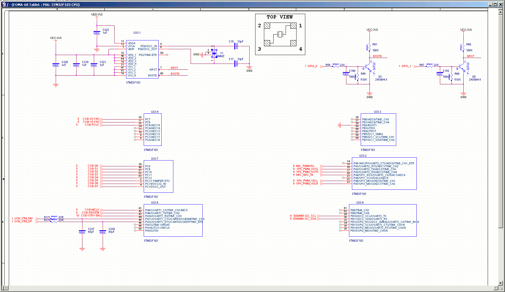
8 Nov 2012: STM32F103 Audio and Camera
Looking at Camera ICs such as the GL860A, it was discovered that these ICs are typically 8-bit micros with DMA. The initial decision to not use the STM32F was therefore reversed, more thoroughly investigated, and found to be workable. Several circuits were tracked down which contain PWM audio volume control, and PCM audio output. These will be added later but for now here is a screenshot of the STM32F showing plenty of pins available to cover all three functions, camera, mic and speakers. It looks like there may also be room (and spare pins) to cover a separate Headphone audio output circuit as well. Sparkfun have a suitable camera (TCM8230MD) which has been proven and demonstrated to work with an STM32F: even the software is already available thanks to the "Following Robot" project by Adam Greg.
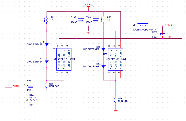
Here is the two audio circuits, one uses a Transconductance Amplifier which can basically be used as a voltage-regulated amplifier. By using a PWM input (through a capacitor) the microphone's volume can be amplified just by using a single pin (in PWM mode) from the STM32F. The second circuit is a straightforward H-Bridge MOSFET amplifier, which again will receive PCM-encoded volume. A low-pass filter turns the amplified PCM output into reasonable audio. By running the PCM at very high frequency (1Mhz) the quality can be greatly improved, however this is only for 1W speakers.
![]()
4 Nov 2012: Schematics started
An initial PCB layout has begun, which will include Mini-PCIe-based USB WIFI. Here is a screenshot showing the Mini-PCIe connector and the power circuit: