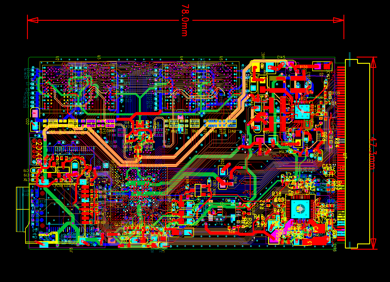
11 Jul 2014: Routing Completed
Here is the first Ingenic EOMA68 CPU Card with the JZ4775. The PCB and Schematics were completed with kind assistance from Ingenic's Engineering Team thanks to provision of EVB Schematics and some much needed and very high quality design advice. Their documentation on design advice is superb and has sections on NAND and DDR design layout that are valuable for general-purpose designs as well as for the JZ4775.
The original EVB PCB Layout was of a much larger demonstration PCB with many more features, connectors and ICs. When transferring to the EOMA-68 47.3mm form-factor it was an extremely tight fit! The DDR3 RAM ICs at the top had address lines routing out almost 8mm above where the PCB currently ends. Several careful days were spent moving these to underneath the DDR3 ICs themselves. Ingenic's EVB PMIC layout was also left pretty much as-is. This saved an enormous amount of development time.
Then, also, the Power Capacitors connected below the SoC (bottom of picture directly below the 4 DDR3 RAM ICs) had to be moved to be positioned to the right of the CPU (4 red and cyan components one above the other). Just to the right of those is an I2C Real-Time Clock IC which also provides a stable 32kHz signal to the SoC. To the right of that (bottom left corner) is a RT8118 Gigabit Ethernet PHY. The top right corner is occupied with an AT8800 PMIC. Various (4) quite large Inductors as big as the PMIC itself may be seen around it.
Storage is provided (bottom left) by a standard 48-pin TSSOP NAND IC as well as a Micro-SD SD/MMC card slot.