10 Dec 2014: Revision 3.2 PCB
A decision was taken to redo the entire PCB layout, after discovering the Hannstar 7in 1280x800 LCD and a 10in 1280x800 from the same manufacturer. A total redesign is required for two reasons. Firstly: the LCDs have completely different pinouts. Secondly - more importantly - the LG 7in display had a PCB 2mm high on the left-hand side but the Hannstar 7in LCD has its LVDS conversion PCB at the bottom. In order to ensure that the thickness of the entire tablet is not increased by the height of the LCD's on-board conversion PCB, it is necessary to completely redo the layout, to a 5.5in x 3.2in PCB.
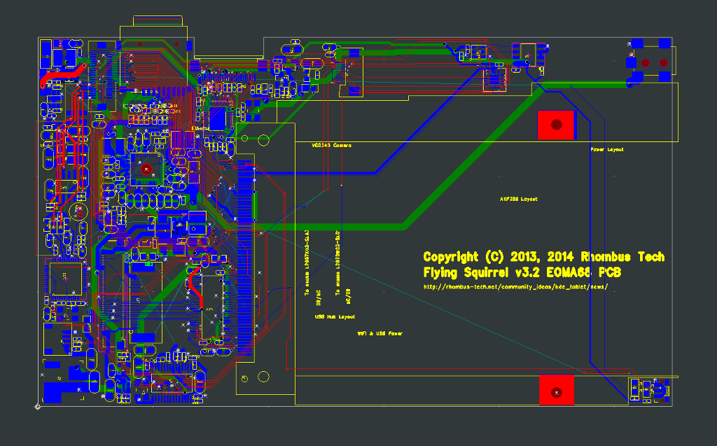
So a decision was taken to make this PCB be useable for a 10in netbook as well as a 10in tablet and a 7in tablet. In order to ensure that the connectors all fit on the left or right edges only, the Headphones, USB and Ethernet have been moved to a separate (small) PCB that will be reached via a 40 pin dual-row 0.4mm pitch B2B connector (top left corner). The Camera IC and Touchpanel connectors have been left in exactly the same relative positions, but this is literally a complete re-layout that is still in progress.
Moving the USB, Headphones and Ethernet to a separate PCB is very handy, as different connectors for a particular purpose may be chosen. For example, as this is quite a thick tablet it is perfectly reasonable to put a full sized USB (A) connector on it, rather than the smaller Mini or Micro USB. Also, for repair purposes, replacing one small PCB is much cheaper than replacing the entire unit, so for that reason moving the DC jack to the smaller PCB is under consideration as well. As there is an on-board AXP209, still, battery charging may take place as well via a USB-OTG socket on a CPU Card (if there is one).