15 Oct 2015: Libre Laptop PCB 3 Power and Battery Charger arrives
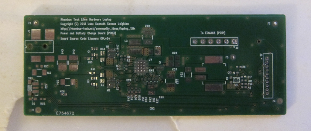
PCB3 arrived today from Eurocircuits (many thanks!): it had been decided to get this one made up with a silkscreen instead of a bare prototype board, because of the size of some of the components (especially the STC3115 battery monitor IC). The wisdom of using such a tiny 3x4 BGA IC may indeed be questioned, here, especially when there is a QFN available, but there is an example PCB layout in the application note that uses the BGA, not the QFN.
The quantity of vias drilled into this small 1.25in x 3.5in board is somewhat stunning. The ampage is somewhat high, though: 4 to 5 amps, so it is essential that the current gets through between layers. Also, just to the north of the LT4156 (centre of the board) is the power inductor, where the output from the LT4156 is operating somewhere around 2mhz. Surrounding the short copper plane between the LT4156 and the power inductor with GND vias is therefore absolutely essential, to the point where vias have been added in between the two inductor's pads!
This is a particularly tricky board: there are areas where there are supposed to be minimalised current leakage, which is hard to do when there are only two layers and the size is so small. Also, the LT4156 QFN only has one GND pin: the centre pad. Twelve (12!) GND vias were placed under it so that the pad would be properly grounded, however the surrounding digital signals had to be reorganised twice to ensure that there was free GND copper on the underside completely surrounding where those 12 vias came out.