20 Aug 2015: First revision Libre Laptop PCB boards
Layout of the three PCBs has progressed very rapidly - far faster than the time taken to develop the casework, by literally an order of magnitude. The boards are being done as 2-layer PCBs. It is amazing to find that the cost of 5 prototype 2-layer PCBs is around $50 for a 48-hour turnaround. Compared to $500 for even a 4-layer PCB that takes over a month to be delivered, the decision to attempt to make all the PCBs as 2-layer makes a lot of sense.
The Laptop's PCBs are divided into three parts, for several reasons. Firstly: to put all the components onto a single 12in-long PCB does not make sense. The shape would be flimsy, awkward to cut, and would have significant void areas. Secondly: the Power PCB for the Battery Charger IC needs to be 2oz copper (it's coping with 15 watts) whereas the rest of the design does not. Thirdly: there are structural dividers and supports in the way, and fourthly: the PCB with the STM32F072 (for a keyboard controller, touchpanel, Real-time Clock and Power Manager) has to be at a different height from the other PCBs. The fact that this allows for a lower cost of development, lower risk, as well as design re-use is almost incidental.
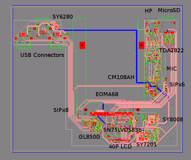
PCB1 contains the EOMA68 CPU Card slot, as well as all the main user-facing I/O: USB ports, USB Audio, LVDS IC for the LCD, Headphone, Mic, speakers, Micro-SD card slot. The USB connectors can be seen in the top left corner: two facing inwards into the interior compartment, and one facing outwards. Micro-SD and Headphone/Mic jack can be seen in the top left. The IC in the middle, below the Headphone jack, is the CM108AH audio IC, and the components in between are mostly the two 0.5 watt TDA2822 amplifiers, for the speakers. They're not hugely powerful, but the power budget isn't big enough to do more (the LTC4155 - the only dual-charge high current single-cell battery charger and power management IC that could be found - is restricted to 15 watts).
Just to the right of the CM108AH is the main power input connector: a 6 pin 2.54mm SIP header. This provides the USB-OTG-style EOMA68 reversible power to (or from) the CPU Card, as well as the main (3A 5V) power for the peripherals. Below that is the 3.3V PMIC circuit (a SY8008), then below that in the bottom left corner is the current-controlled step-up converter for the LCD backlight. This IC is a SY7201, but there are also some transistors next to it which regulate the Digital I/O Power to the LCD, as well.
To the right of the SY7201 is the 40-pin LVDS connector to the LCD, and above that is the SN75LVDS83B - a tried-and-tested RGB/TTL to single channel LVDS converter IC from Texas Instruments. The design of this IC is amazing: it is clearly well laid out so that it can be placed close to both its source and sink. The fact that its digital I/O side can be anything from 1.8 to 3.3 volts is also incredibly useful, in the circumstances where the CPU Cards in the future may go down to 1.8v signals. VREFTTL (from the CPU Card) is there for exactly this purpose: VREFTTL is connected directly to the Digital I/O Power on the SN75LVDS83B, and as a result there are no level-shifting ICs needed.
In the bottom left corner is a standard GL850G 4-port USB Hub. With quite a lot of reorganising and a lot of care, it has been possible to arrange all the USB differential pair signals (with the exception of a very short cross-over leading into the USB hub) on the top layer, leading directly to their connectors, and, crucially, with virtually no signals crossing under them on the 2nd layer. The layout is slightly odd as a result, but it was considered to be the highest priority, to ensure that the USB differential pairs have as little interference as possible.
Just above the GL850G can be seen an 8-pin 1.27mm SIP header. This is for connecting to the STM32F072 board. Power is provided, USB connections (to the second EOMA68 USB port), and three GPIOs are connected up. First is the EOMA68 "Reset / Power" - this goes straight to an STM32F072 GPIO. Second and third are the BOOT0 and NRESET lines of the STM32F072. Thus, although the STM32F072 controls the power-up status of the EOMA68 CPU Card, the EOMA68 CPU Card also controls the STM32F072, and may be used to reset it and re-flash its firmware. In this way, the EOMA68 CPU Card can be used to develop and test new firmware for the STM32F Embedded Controller.
The final IC to mention is the SY6280, which is just next to the USB2 ports at the top left. This is a current-limiting IC where the limit has been set to 1.25A. This is not precisely within the specification of 3 USB ports (which should be 1.5A) but the power budget for the LTC4155 is being pushed very hard, as is the SY6280. The SY6280's "enable" state, like all the other Power ICs, is controlled by the EOMA68 CPU Card GPIO. The only IC not under direct power control is the CM108AH: this is supplied directly by 5V system power, as it is primarily designed to be operated from a 5V supply, not 3.3v.
A decision has been made to minimise components, here, as well as complexity. Power-up GPIOs are shared in some cases (for example the LCD power-up GPIO controls the Digital I/O as well as the Analog Backlight power). If this was not done, then an extra IC (I2C GPIO) would be needed, which would then necessitate a linux kernel driver as well as a more complex GPIO structure.
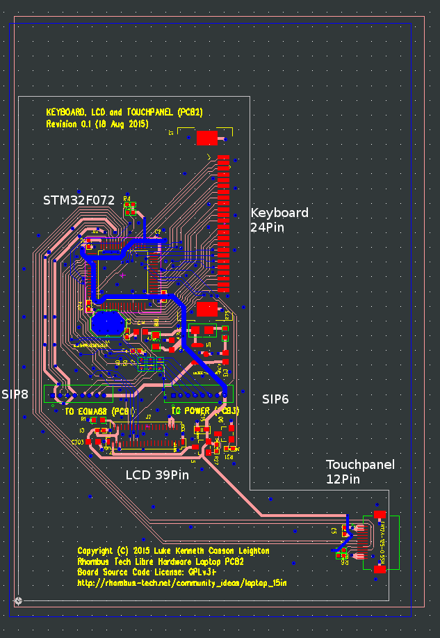
The second PCB is the keyboard, touchpanel, panel LCD, power controller and Real-time Clock board, using a 64-pin LQFP STM32F072RB which has a built-in (accurate) main crystal. The built-in crystal not only saves on complexity as well as cost, but also on space. Amazingly, for such a simple-looking board, space for routing has turned out to be very tight, due to it being only 2 layers.
Originally it was naively believed that the lower-cost ($1) 48-pin STM32F070 could be used, but it turns out that this was a hopelessly overoptimistic idea! The GPIO pins to the STM32F072 turn out to be: 24 for the keyboard, 4 for the touchpanel, 6 to the Power PCB (!), 5 to the main EOMA68 PCB, 6 to the LCD. That totals 45 pins already! There are 10 for power, 2 for the 32.768kHz real-time clock crystal: the actual total number of spare pins left is now only two easily-useable GPIO pins!
The keyboard connector is a 1mm pitch 24-pin FPC. The matrix has been mapped out and turns out to be a 16x8 (16 input, 8 out). The connector is in the top left of the picture, below. The STM32F072 is in the top middle. Directly below it are the SIP 8-pin connector (which goes to the GPIO of the EOMA68 board, with the USB connection and reset lines), and the 6-pin SIP connector that goes to the Power PCB. The Power PCB connector links to the I2C bus of the two ICs on it, for monitoring both battery charge and battery capacity. Below the two SIP connectors is the 39-pin 0.3mm pitch LCD connector: this is a very fine pitch connector that has to be exactly in the right place, to fit the very specific (Yunlea) LCD connector. At the far bottom left corner, again in a very specific location to fit the Yunlea LCD, is the touchpanel FPC 12-pin connector.
Positioning of all three FPC connectors is very tight and has to be exact. Also, the SIP headers need to be right-angle and need to be soldered on the underside of the PCB, so that the headers come out just in the available space underneath the LCD casework. The pins, protruding out the other side, have been accounted for in the design of the touchpanel holder.
The nice thing about this PCB is that it could potentially be utilised in a stand-alone product: a USB-powered keyboard with touchpanel and LCD attached. The STM32F072 can scan the keyboard and receive the I2C touchpanel signals, and convert to USB-HID keyboard and mouse events. Also, the backlit LCD makes a cool way to interact with users, allowing presentation of icons, buttons, prompts, alerts, scrollbars, drawings - even small games if desired.
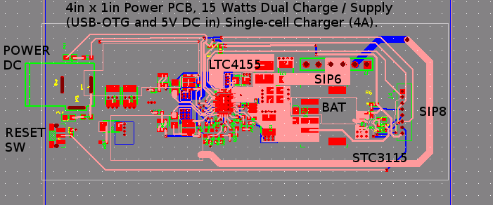
Below is the Power PCB. This board has to be 2oz copper because the amount of heat is considerable: 15 watts. The board is therefore larger than it appears, so that the copper on the PCB can act as a heat spreader. There are only 2 ICs: the LTC 4155 and the STC 3115. The STC 3115 is a "battery capacity" monitor IC that measures both voltage and current, and "learns" the battery's state over time. The LTC 4155 is a single-cell charging IC that can handle up to 4 Amps charging, and it can supply a total up to 3 Amps at 5V to either the USB-OTG or to the "System" output. Also, it can switch to USB-OTG "power in", and can take power from there, to supply it as "System" output and also for battery charging.
So the LTC 4155 is the perfect IC for EOMA68, being higher current than the X-Powers AXP209 and even the more recent X-Powers PMICs like the AXP221. The X-Powers AXP series of PMICs have a much better range of outputs that can be controlled via I2C if desired, including LDOs as well as DC-DC converters, but in this particular design, the X-Powers PMICs simply can't handle as much current at 5V as is required for this laptop, nor can they handle 4A charging for 10Ah batteries, and the range of LDO outputs and DC-DC conversion simply isn't needed. The only voltages needed for the 15in Libre Laptop are 5V and 3.3V, the 3.3V being needed for the STM32F, the MicroSD card, the LCD Backlight and the GL850G, whilst the 5V is needed for the USB connectors, USB Audio and the speakers. With the 3.3v regulator being on the main EOMA68 CPU Card PCB, a plain and simple 5V system output (and a USB-OTG-style bi-directional supply) is all that's needed.
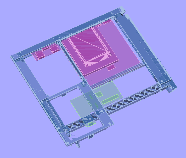
Lastly it's worthwhile showing an OpenSCAD rendition of PCB1 and PCB2 in place. These were originally modelled with pyopenscad as "cubes", so the components positioning could be more accurately assessed. It was not an automatic process turning those 3D positions into IC positions on the PCB design, so to double-check the PCBs will be prototyped (at a cost of only around $50!) and the positions confirmed prior to actual assembly.