23 Mar 2013: Rapid progress
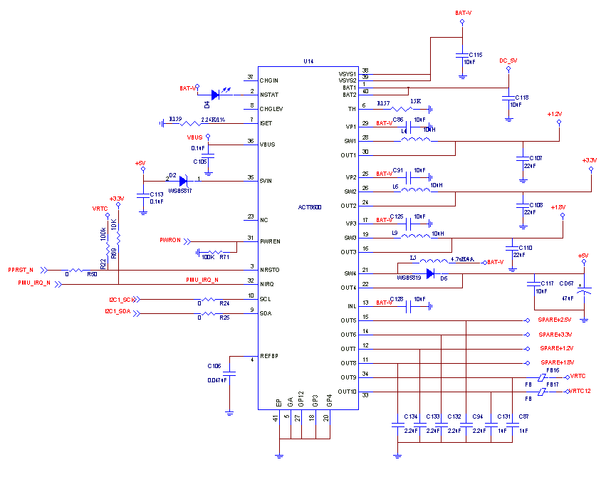
Well. amazing. Ingenic provided a review of the schematics, free of charge, spotting 10 errors and giving invaluable advice. This board is actually much much simpler than the other two, most notably because it only has two RAM ICs, freeing up considerable space despite needing an Ethernet Controller, USB Hub and a JM20327 USB-to-SATA converter. ACT do absolutely fantastic PMICs - the ACT8600 as well as the ACT8930 would be absolutely perfect... except that they are not very common, and the MOQ is for 10,000. So a decision had to be made to return to using the same easy-to-find generic SOT23-5 parts that were used in the Ingenic JZ4760 LEPUS reference design.
Some considerable effort has been expended to track down a Gigabit Ethernet Controller IC. These are extremely rare. The only one located is a 16/32-bit one from ASIX, the AX88100. Unfortunately, this controller, listed as "non-PCI", is a bus-to-GMII/RGMII converter, meaning that an additional chip is needed - a RGMII PHY. The AX88100 is already a 128-pin QFP, and RGMII PHYs are quite a few pins as well. Additionally, the AX88100 has to run at 125mhz and the combination with the PHY chip turn out quite a bit of heat. So, reluctantly, the DM9000 looks like it is the best option: lower power, smaller size (it's only a 48-pin QFP) because it drives Ethernet Tx+/- and Rx+/- lines directly itself.
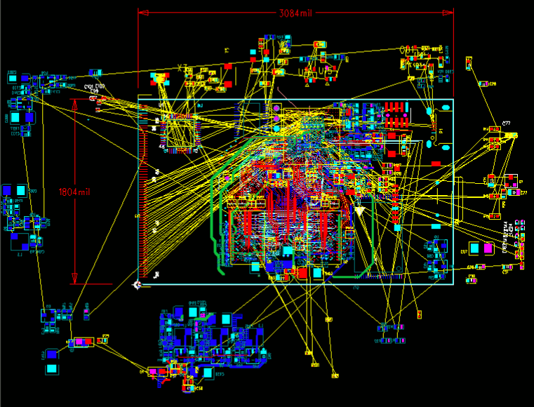
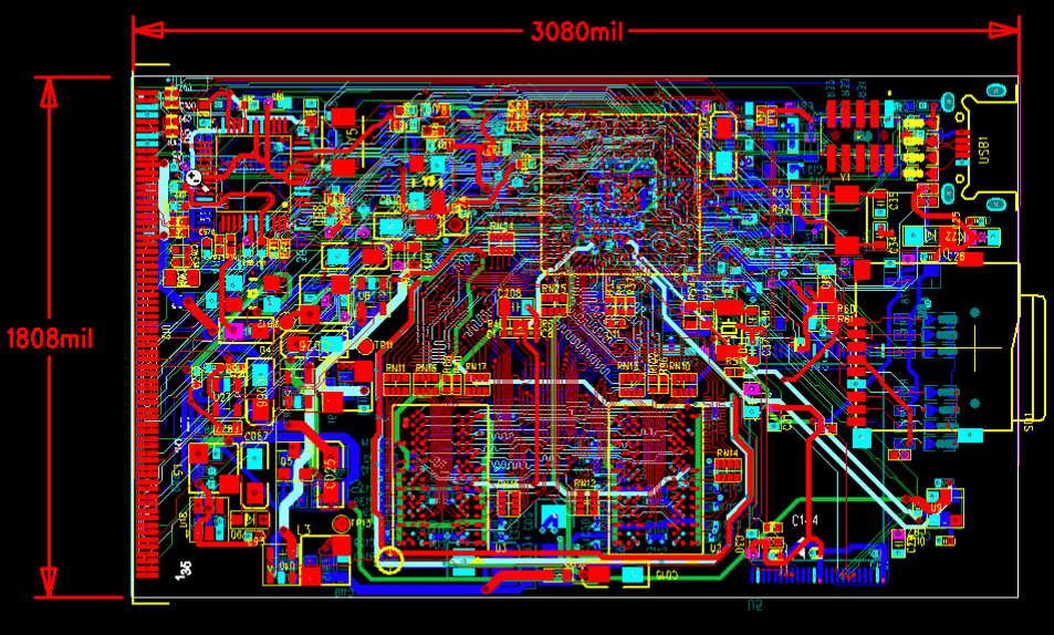
The board below is progressing nicely: auto-routing took only 7 minutes to complete including optimisation, which is very very fast: the iMX6 board takes between 25 and 45. Possibly the lack of HDMI output makes this board that much easier; also the CPU is only 328 BGA pins, 17mm sq whereas the A10 is 424 and 19 sq mm. Next up will be to put in some power planes: the LEPUS board's layout doesn't have any. Also, some help and advice would be greatly appreciated for the SATA and Ethernet planes and E.M. shielding. One thing worth noting: there has to be a better way to do keep-out around the DDR2. The track density on the DDR2 area isn't high enough to stop the auto-router from trying to route other tracks through it. To stop that from happening, it has been necessary to surround the DDR2 - on each plane - with a GND track! Anyone with experience of PCB design will immediately know how to do this better.
18 Mar 2013: First run of the auto-router
Preliminary placement of the compoents is successful! Routing has to begin some time, so a quick auto-route was carried out. All but 12 out of 1,000 connections requiring completion were connected on the first run. However, as can be seen, no Design Rules or Copper Pour has been added for the Power lines, which will be the next main task. As a general rule, however, the layout of this board has been very straightforward, due in part to finding the ACT9000 PMIC which has left plenty of space. By contrast the iMX6 PCB is incredibly busy (discrete ICs for each Power line), and the A10 PCB was very close to the limit as well.
17 Mar 2013: Schematics found using ACT9000 PMIC
An accidental find - the schematics for the Ingenic JZ4780 - included references to a Power Management IC (similar to the A10's AXP209), called an ACT9000. This PMIC is a TQFN55 (40 pin), with an exposed pad just like the AXP209 (QFP-48), and it is only 5mm square. The inductors, of which there are five (one for each power line) are about the same size! The ACT9000 replaces about six or seven discrete Power ICs, most of them SOT-25 packages, thus greatly simplifying the schematics and allowing it to fit into a smaller space. This Is Good.
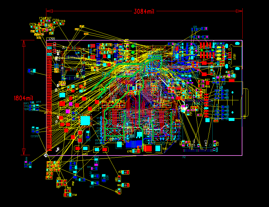
Layout is progressing: components can be seen to be migrating in slowly. Top left is the USB-to-SATA JM20329, with the DM9000 Ethernet Controller overlapping. (Note: if there was a low-cost easy-to-find Gigabit Ethernet Controller with an 8 or 16-bit memory interface, now would be a good time to find one). Top Centre is the jz4760; Bottom Centre are the two 16-bit-wide DDR2 RAM ICs. To the left of the CPU is a boot selection jumper; to the left of that is an FE1.1 4-port USB Hub which substitutes for the unfortunate lack of USB 2 interfaces on the jz4760. Top right is the MicroUSB interface; to the left of that is a JTAG port which will be unpopulated in production. Micro-SD is centre right. Bottom right is a big empty space where Micro HDMI should be, if it wasn't for the inconvenience of tracking down and also having an extra IC for HDMI conversion. Overlapping the MicroSD is the single NAND IC. Overall the layout is fairly similar to the iMX6 EOMA-68 CPU Card.
16 Mar 2013: Ingenic JZ4760 CPU Card begins
Many thanks to Ingenic for providing reference schematics and PCB layout files for the JZ4760. The JZ4760 was chosen over the JZ4770 and the JZ4780 because it is FSF-Endorseable. The JZ4760 does not have SATA, and only one 480mbit/sec USB interface: the other is USB 1.1 so a 4-port Hub has to be added, to which a JMicron USB-to-SATA interface has been added. In combination with the JZ4760 having a limitation of 512mb DDR2 RAM, it is only because of FSF Endorseability that the use of this processor makes sense. The aim here is to provide people who honour Software Freedom with a way to contribute to the goals of the EOMA Project, and to have access to and be able to influence the design of modern products at the same time.
Preliminary PCB layout has started, and can be seen below. Ingenic's reference schematics are at the heart of this layout, with the CPU and the DDR2 RAM, tracks and support components being left entirely alone. The Power ICs will need to be re-laid-out, and remaining components slotted in. NAND Flash and the Mid-Mount connectors from other EOMA-68 projects have been added as well. Although an HDMI interface could be added, it requires yet another IC in order to do it, and there is no separate framebuffer. To save cost, and make the PCB practical, HDMI is not being added. SATA is being supported as a USB-to-SATA IC - the JM20329.