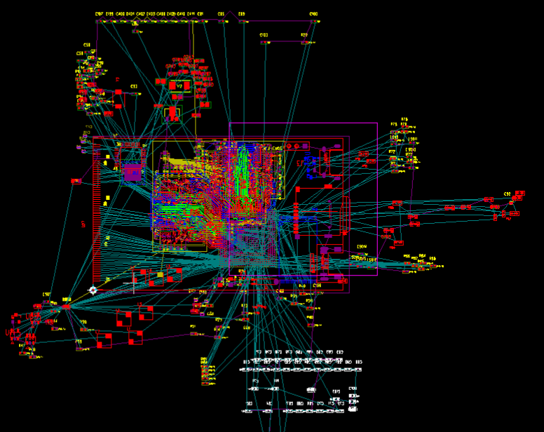
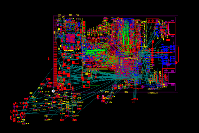
4 Apr 2013: Preliminary PCB layout: components fit
With some guesses as to the size of the AXP221, the layout has been roughly completed, components placed, and power planes begun. Manual work on laying out copper pads for the AXP221 cannot begin however until its size is confirmed. However there is still quite a lot left to do, such as setting up the Design Rules for the auto router to complete the LCD, HDMI, NAND, SD, SATA. Ethernet etc. This is also progressing well.
4 Apr 2013: Preliminary PCB layout nearly completed
Approximate layout (placement) almost done - the bit that's missing is the AXP221. With no datasheet or PADS layout that's the main thing which is holding things up. With little experience at this, it's hard to tell if the idea of overlapping the SATA IC with the Ethernet IC is a good idea. We shall see!
31 Mar 2013: Schematics, PCB layout and GPL Source code received
After discovering the low-cost JM20329 USB-to-SATA IC, the creation of an A31 EOMA-68 CPU Card made a lot of sense. A request to Allwinner for example schematics, PCB layout for the DDR3 RAM section, GPL kernel source code and u-boot source code was sorted out within under 24 hours - thank you!
Due to the parts having been sourced and the parts created for other projects, the first revision of the A10 EOMA-68 Schematics was sorted out in a little under four hours. The PCB will however take a little longer!
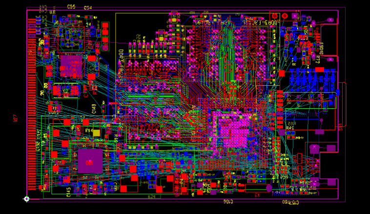
2 Apr 2013: PCB layout started
A very rough layout has begun, and the process of synchronising the PCB layout with the schematics has started. Approximate positioning shows already that this is achievable, although it may be a little tight on the PMIC side. The bottom left corner is reserved for the AXP221. The connectors are to be placed in exactly the same locations as for the A10/20 and iMX6 CPU Cards.
Thanks to Allwinner for providing the DDR3 RAM layout, this CPU Card will have four 16-bit-wide DDR3 RAM ICs, in two separate banks providing a total 64-bit-wide memory access (similar to the iMX6 CPU Card). The provision of this pre-tested layout will greatly accelerate the time to completion of the PCB.