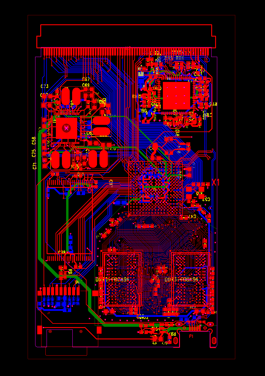
31 Jul 2014: Main routing completed
The main GPIO and other routing is now completed, leaving just the power planes to do. It is noted that the pinouts for the A33 have been designed very carefully: note that the majority of the NAND pinouts go directly on a single layer between the CPU and the TSOP-48 NAND IC (left middle: red lines). Likewise the RGB/TTL BGA pin placement has been extremely well thought-out, so that the tracks in blue (to top left corner) could likely be done almost with very little cross-over. However, as long as this layout is functional it need not be fine-tuned to such an extent. It's quite exciting that this PCB is progressing so rapidly!