15 Jan 2013: 2nd attempt at a PCB layout
The "no idea how to do this, maybe it will save time and costs and it's fun anyway" PCB layout is progressing well: it's now down to 125 x 113mm (5 x 4.5in) and contains approximations of the various components (PCB Decals) which a professional PCB designer should at least be able to run with. Experimentation with the Auto-router has been fun and games: it's not perfect, but laying out some parts by hand (including the VCC-3V3 and VCC-5V0 lines), the RGB/TTL portions and the AXP209 fan-out has got round most of its weaknesses.
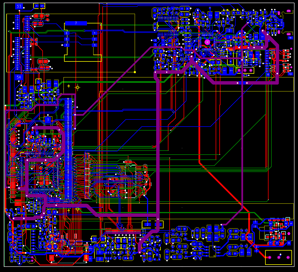
Component positioning has been an interesting part of the experimentation. Top-left is the USB-based Mini PCIe, with a Litkconn SIM Card holder underneath. The FE 1.1 USB Hub fits top-centre. The AXP209 and the majority of the power conversion circuits fit top left, and the Micro-USB and Micro-SD fit in the very top left corner. The 100-pin STM32F is in the middle of the left side: it's a tight fit. The 5V Power In connector hasn't been done yet: it's in the bottom-right corner and a large 3-pin SIP connector has been chosen as a temporary substitute. Next to that is the Audio jack: speaker headers just to its left. In the far bottom left corner is the Microphone. To the right of that is the CSI Camera Interface; to the right of that is the LVDS connector for the 1024x600 IPS LCD Panel.
To the immediate right of the STM32F, a 60-pin expansion header was chosen as it saves a great deal of space: this connector will allow the exact same PCB to be used in a larger device including a low-power laptop. The pin-outs include 20 STM32F pins (for use as a keyboard matrix), Ethernet and SATA. Potentially there is room to route the GPIO pins from the AXP209 as well, just... because they're there.
The actual layout has been quite straightforward: using "grouping" has allowed the components to be moved about conveniently, as well as allowing their Net lists to be selected and specific track widths applied. The majority of components, despite the small size, have been kept on TOP in order to ensure that there is good clearance for the LCD Panel. Potentially, with a small increase in length in order to accomodate the Expansion Header, all components could actually be moved to TOP, thus reducing the manufacturing costs. The kicker will be the LVDS Panel, as a cable would be needed which folds back and reaches the other side.