10 Nov 2013: Third revision finalised
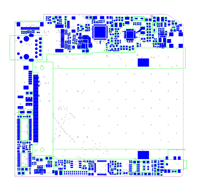
The revision 3 gerbers have gone to the factory to be analysed. If they pass inspection then some sample PCBs will be made up and populated. For what appears to be such a simple task - "make a tablet PCB" - this is an amazing amount of fuss, and very little spare space! The PCB is around 10cm square yet there is no room for additional components.
Partly this is down to it being entirely single-sided, partly due to optional capabilities for alternative purposes. The reason for the board being single sided is not so much to reduce cost (which will be an interesting side-effect) but because the 6mm PCMCIA socket is already too much for an extra 2mm clearance of double-sided components to be acceptable. When in a case the product will come out at just under 13mm. 6 for the PCMCIA socket, 1.2 for the PCB, 3mm for the LCD, 1.5 for the touch screen glass and 1mm for the plastic casework. Alternative materials such as magnesium alloy have been considered, in order to get the thickness down. Still, the critical part is the PCB: let's see how that works out.