1 Nov 2013: Third revision routing
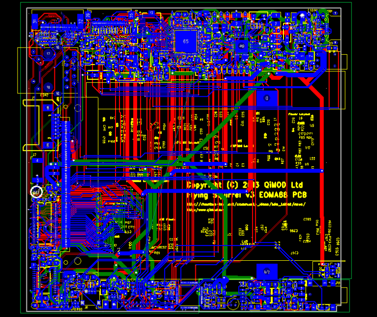
With some help and guidance from a lot of people, on design rules and PCB layout, the routing is progressing. The auto-router simply doesn't cut it on the differential pairs, so these have been initially laid out by hand, then allowed to be resized (length-wise). Likewise after several false starts a decision was taken to route the RGB/TTL by hand as well. Although the auto-router could make the connections with some hints, it just looked dreadful.
Also the PCB Factory have been very helpful, asking the right kinds of questions that lead to exploration of "impedance" for example. So many details to deal with! Many thanks to Ryan for the hints about only allowing 90-degree entry into square pads: this has got rid of more design flaws than anything else.
The QFN and the LCD connector pad sizes are tiny. The AXP209's clearance is only 5.8mil. Also, it's incredibly densely packed. So, surprisingly, even though this is "only" an I/O Board, minimum track width has had to be cut to 6mil, and track-to-track of 5.5mil has had to be allowed.
Also a nice addition: it turns out that the 1024x768 LP097X02-SLA3 LCD is not a million miles different from the LD070WS01 in terms of connections. Several (20!) 0R resistors have just about fit under the connector, making it possible to try a 9in 1024x768 LCD out on this board.