07 Mar 2017: First revision EOMA68-RK3288 CPU Card PCB testing report
So, a combination of strange things from testing: firstly, that the RK3288 can in fact be successfully booted from USB, but that when doing so it is placed into a special mode that excludes the possibility of running more than one single process, and SMP mode is also prohibited. This took a number of days to work out. Secondly: it is possible to drop the clock rate of the Samsung 1600mhz DDR3L RAM right down to a clock rate of only 200mhz, but when doing so the board will not be able to read (boot) from external MicroSD - not when using u-boot, at least. Only when initialising the RAM speed to 300mhz or above does MicroSD boot proceed further. The exact reason yet is unclear.
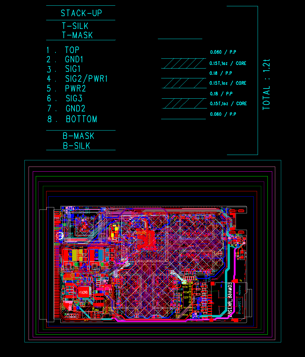
However what does work is the (proprietary) rockchip 200mhz DDR3 initialisation binary, which has proven extremely useful but ultimately cannot be utilised (proprietary binaries). Part of the problem is that whilst most PCBs developed so far are 1.6mm FR4 (standard epoxy / fibreglass) and 6 layer, the EOMA68-RK3288 is only 1.2mm and is 8-layer. That reduces the distance between the layers from 10mil to only 6mil (6 1,000ths of an inch) which is absolutely tiny. It also changes the impedance of the DDR3 tracks from the Reference Design's (estimated) 90-100 ohms down to half that amount: around 50 ohms.
Now, thanks (again) to the input from #rockchip-linux paulk and ayaka
kindly pointed me in the right direction: it's possible for these DDR3
RAM Controllers to change the impedance of their line-drivers and receivers.
So that's the first thing that will be investigated tomorrow. Looking
in u-boot-rockchip source it turns out that the impedance is actually
hard-coded  to 40 ohms driving and 155 ohms termination. Normally
the controller is asked to carry out auto-impedance matching: it seems that
in the standard u-boot-rockchip source this has been disabled! That would
be perfectly fine if the PCB being developed was anything remotely close
to the stack of, for example, the Firefly, but it's most definitely not.
At least however there is a way forward: something to continue trying,
rather than give up on $USD 1500 worth of prototype hardware.
to 40 ohms driving and 155 ohms termination. Normally
the controller is asked to carry out auto-impedance matching: it seems that
in the standard u-boot-rockchip source this has been disabled! That would
be perfectly fine if the PCB being developed was anything remotely close
to the stack of, for example, the Firefly, but it's most definitely not.
At least however there is a way forward: something to continue trying,
rather than give up on $USD 1500 worth of prototype hardware.
Update 2017mar12: found the following settings which could match the (almost 50 ohm) impedance of the EOMA68-RK3288 PCB, to be tested shortly:
    /* http://www.skhynix.com/product/filedata/fileDownload.do?seq=6790
       MR1: bits 9,6,2 = b001 = RZQ/4 = 60 ohms ODT
            bits 4,3   = b00  = CAS disabled
            bits 5,1   = b00  = RZQ/6 = 40 ohms output driver impedance
            bit  7     = 0    = write-leveling disabled
            bit  11    = 0    = TDQS disabled
            bit  12    = 0    = output disabling not enabled
            bit  10    reserved
            bit  8     reserved
       MR2: bits 10,9  = b01  = RZQ/4 = 60 ohms ODT
            bits 6,5,4 = b001 = CAS Write Latency 6
            bits 3,2,1 = b100 = partial array self-refresh 3/4 array
17 Feb 2017: First revision EOMA68-RK3288 CPU Card PCB assembled
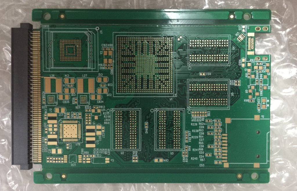
The components have all been placed onto 5 PCBs, with the exception of the RK3288, RAM ICs and eMMC. Two of the PCBs have been fully assembled with an RK3288 and the 4 DDR3 RAM ICs. The first PCB was not successful in being recognised on the USB-OTG bus. Power was all okay, but there was no activity on either the eMMC or MicroSD clock line during power-up, and the USB-OTG was not responding. Turns out that the OTG port was mis-labelled as the 2nd USB (Host) and vice-versa, so tomorrow's task will be to try using the correct port before proceeding further. Also the PCMCIA break-out board arrived so it has been possible to test using that.
Assembling these PCBs has been exciting as it's been done entirely using equipment in Taiwan in a "home office" environment. A small commercial pick-and-place machine was used, which is due to be replaced by an OpenPNP design. The cost of 10 8-layer PCBs here in Taiwan was only $USD 600, which is about 20% less than the cost in China. Amaazingly, using a small IR oven, the 600-pin 0.6mm pitch BGA RK3288 IC was successfully soldered on. Even the tiny 20-pin 0.5mm pitch 1.8mm x 2.0mm 3A PMICs were successful. It is a fascinating process to watch and experience. Photos to be included in this update, later.
19Feb2017: first board, memory isn't initialising at full speed: setting DDR3 clock rate down to 200mhz successfully completes DDR3 initialisation: moving on to mmc initialisation that fails spuriously which generally indicates memory unreliability. attempting the bootup with a second board.
12 Jan 2017: First revision EOMA68-RK3288 CPU Card PCB made
The RK3288 boards have arrived (qty 10), and they look really good. This is quite an exciting and significant upgrade: the RAM ICs are $USD 10 EACH to make up to 4GB of RAM, bringing the cost just in RAM alone to more than the full manufacturing and testing cost of the EOMA68-A20 boards. The RK3288 is the SoC that has been shown to outperform the latest Intel Atom budget processors. With ultra-fast eMMC it will be very interesting to see what happens.
19 Nov 2016: First revision EOMA68-RK3288 CPU Card PCB Design
The RK3288 was found last week, and a quick search online found a seller on taobao.com willing to provide PADS 9.5 PCB and SCH files for a mere $USD 24. Research showed that the RK3288 is capable of addressing up to 4GB of RAM, which makes it significantly worthwhile pursuing over every single previous SoC ever evaluated. However it has to be done as four 96FBGA DDR3 16-bit wide RAM ICs (if the cost is to be reasonable).
The PCB design that was found was based on a Reference Design from Rockchip, which has two RAM ICs to the right and two below. Total area is around 40mm square (centre of picture, below). EOMA68 PCBs are 78.1mm by 47.3mm, leaving an extraordinarily (ridiculously) small remaining amount of space, and because the main pre-arranged layout is for DDR3 it is not permitted to cross any unrelated GPIO or power tracks through that area. Therefore, there is a scant 4mm above and around 2.5mm below where tracks to the HDMI and MicroSD Card can be routed (right hand side of picture below). Not only that but the Power Management layout barely fits into the remaining space (left third of the PCB), with the eMMC NAND flash IC occupying the top left corner.
The original design was 6 layer: it turned out to be hopelessly optimistic to expect to get all the GPIO routing into 6 layers (and still expect to have a PCB where the Ground Planes are respectable). Adding the extra two layers makes it much easier, much more likely that the design will work, especially given the complexity and compactness of some of the Power routing.
With assistance from #linux-rockchip on freenode it's been possible to get this PCB and schematics done in around ten days. After a comprehensive review it can go to PCB manufacturing and assembly.