19 Nov 2016: First revision EOMA68-RK3288 CPU Card PCB Design
The RK3288 was found last week, and a quick search online found a seller on taobao.com willing to provide PADS 9.5 PCB and SCH files for a mere $USD 24. Research showed that the RK3288 is capable of addressing up to 4GB of RAM, which makes it significantly worthwhile pursuing over every single previous SoC ever evaluated. However it has to be done as four 96FBGA DDR3 16-bit wide RAM ICs (if the cost is to be reasonable).
The PCB design that was found was based on a Reference Design from Rockchip, which has two RAM ICs to the right and two below. Total area is around 40mm square (centre of picture, below). EOMA68 PCBs are 78.1mm by 47.3mm, leaving an extraordinarily (ridiculously) small remaining amount of space, and because the main pre-arranged layout is for DDR3 it is not permitted to cross any unrelated GPIO or power tracks through that area. Therefore, there is a scant 4mm above and around 2.5mm below where tracks to the HDMI and MicroSD Card can be routed (right hand side of picture below). Not only that but the Power Management layout barely fits into the remaining space (left third of the PCB), with the eMMC NAND flash IC occupying the top left corner.
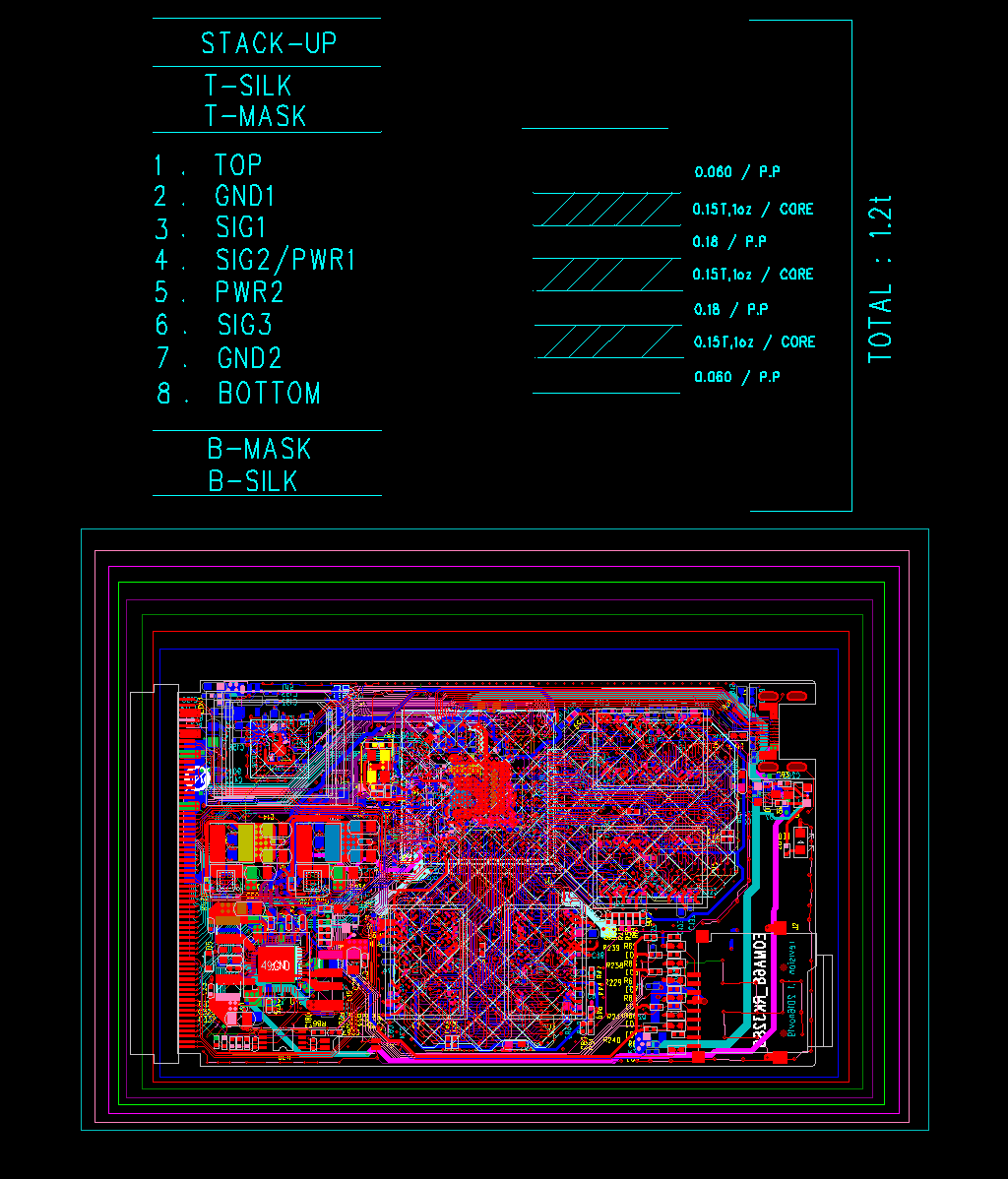
The original design was 6 layer: it turned out to be hopelessly optimistic to expect to get all the GPIO routing into 6 layers (and still expect to have a PCB where the Ground Planes are respectable). Adding the extra two layers makes it much easier, much more likely that the design will work, especially given the complexity and compactness of some of the Power routing.
With assistance from #linux-rockchip on freenode it's been possible to get this PCB and schematics done in around ten days. After a comprehensive review it can go to PCB manufacturing and assembly.