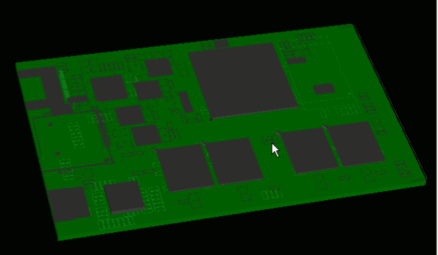
16 Sep 2017: EOMA68-A20 2.7.5 HDMI Final Review
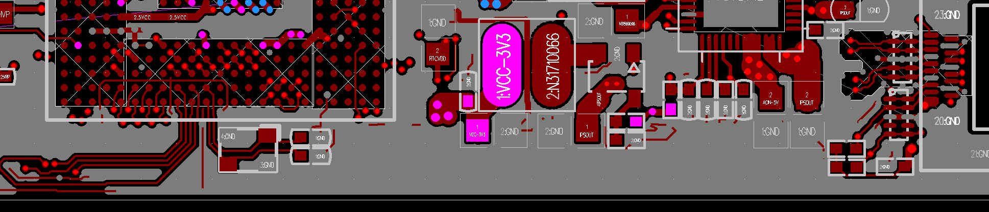
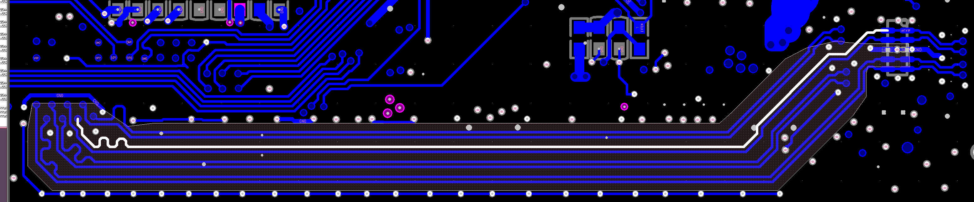
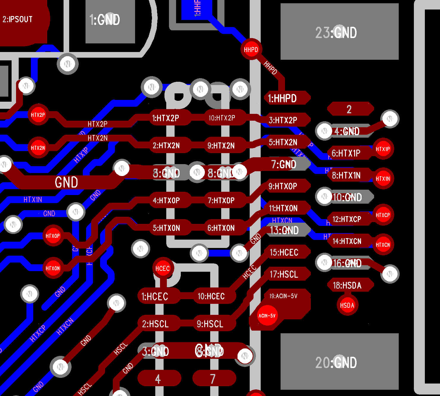
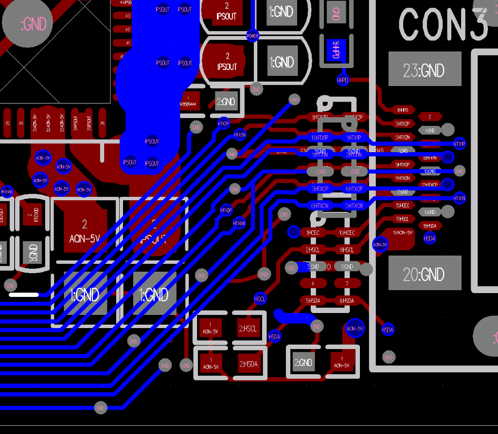
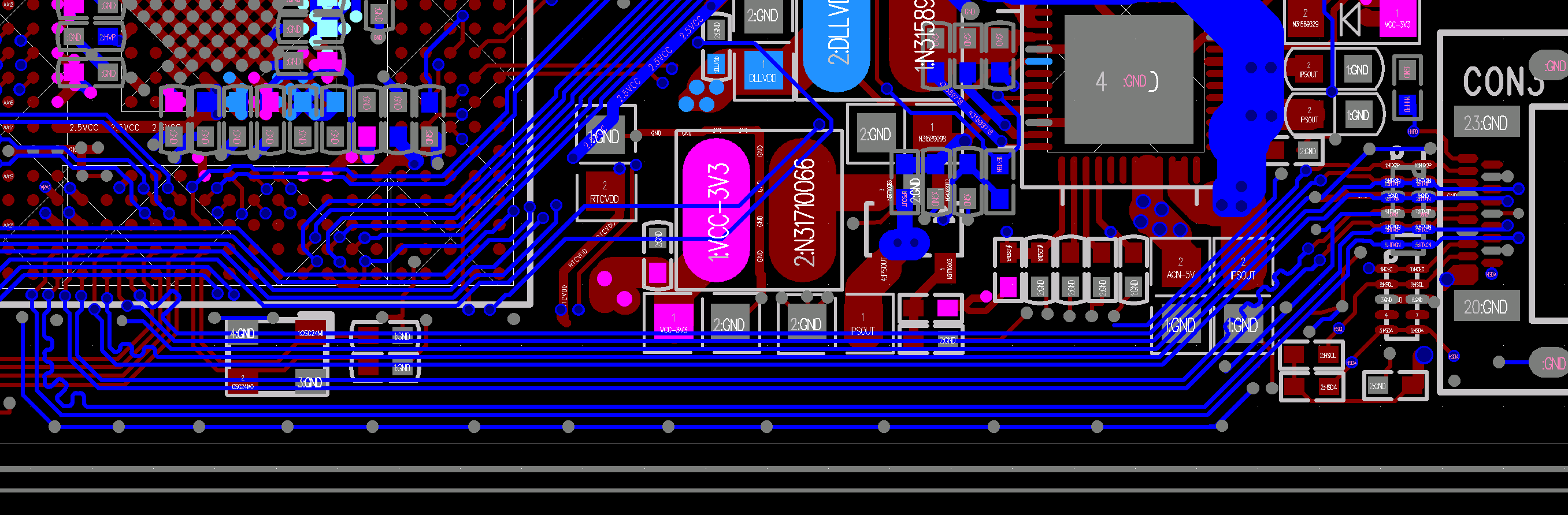
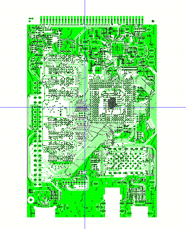
With the DC3 test PCB coming back successful it's time for the last review prior to sending off the gerbers. The main layers are 1 (TOP) and 6 (BOTTOM) however 3 is also included for completeness, also to show how the HDMI signals cross through in a group and form a hole in the GND flood-fill.
Ongoing discussion is here as new images are added.
12 Sep 2017: EOMA68-A20 Pre-Revision 2.7.5 HDMI Test PCB success
So the test PCB to confirm that the very unusual JAE Mid-mount Micro-HDMI Connector Type D, would fit and properly connect up on the tracks without solder wicking away down small VIA holes, has come back a success. 10 low cost test boards were deliberately put through the full manufacturing (solder reflow) process rather than hand-assembled with a hot-air gun, so as to confirm that this extramely small pitch connector would work, and it did.
It will now be possible to proceed with a pre-production run of the 2.7.5 PCBs, with confidence that unlike with the 2.7.4 design there will be a reasonable manufacturing yield. It is unfortunate but not foreseeble or avoidable that it cost nearly $USD 2,000 (10 2.7.4 PCBs fully assembled) to learn that the JAE DC3 connector would not seat properly, however at least the cost of learning that it can be done was minimised by creating a low-cost 2-layer test PCB instead of risking another $USD 2,000 on a full board.
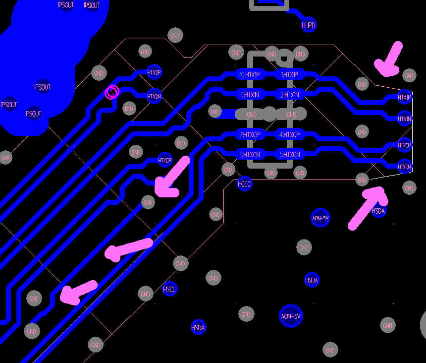
24 Aug 2017: EOMA68-A20 Revision 2.7.5: HDMI Connector Review
So this month's mailing list has been pretty much dominated by the HDMI High Frequency Layout" discussion. The level of detail is incredible, thanks to Richard's input and with others pitching in, it's been amazingly invaluable. Research into best practices, looking up how many bits of latency can be corrected on the signal wires, looking up intra-pair (between two wires) and inter-pair (between pairs of wires) skew calculations, acceptable cross-talk distances, explaining what the difference is between common ground and... the other type... it's a level of detail that's overwhelming.
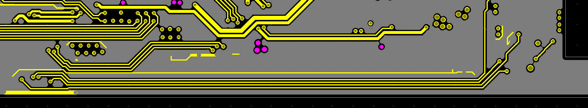
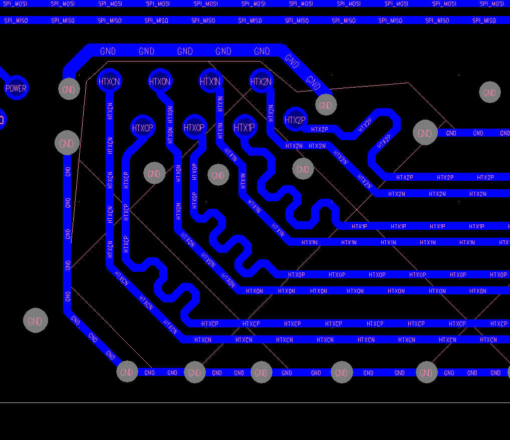
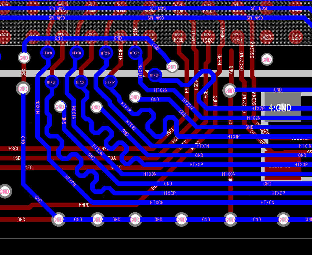
The tracks start out from the processor on the bottom layer (red), and immediately go down to a pair of vias within a distance of only 0.6mm. As best is possible these VIAs have been spaced equally apart and those very short red tracks arranged so that the differential signals come out of the VIAs (up to the top layer in blue) at the exact same time. This results in better signal "cancellation" and you get no EM radiation. Right next to them are GND vias which help soak up any stray noise. Richard understands this stuff best: something about capacitance and inductance vaguely rushed past which made sense.
Also it's critical to note: the signal goes in straight and then comes out straight from the VIA, as best as is possible. A prior revision had the angle of layer 1 (in) and layer 6 (out) at 90 degrees, and in one case 180 degrees (on a single VIA). That had to go.
From there it is rather unfortunate that a right turn is needed. It is unfortunate because the VIAs have to be staggered as they are (because of the red track length-matching) but then that means that there is now an extra 0.25mm to make up on each left track when turning the corner. Normally on a 90 degree turn only a small "wiggle" is needed: each track now unfortunately needs at least two "wiggles" to make it round the corner and remain in "sync". It's not possible to swap the tracks over so that the "N" comes out on the right of the "P" because that would mean that a swap-over would also be needed later on, and that makes a mess near the connector. Also, the space is ridiculously small, and that's the 24mhz main CPU Crystal just half out of picture on the left, so it's very important to keep these 350mhz signal pairs well away from that.
After several sets of wiggles the signals now have intra-pair skew of only a maximum of around 0.03 mil (thousandths of an inch), thanks to getting as close as possible with the CAD software on its current snap-to-grid setting, then finding a corner on the other track and stretching it to adjust to the nearest 0.02 mil. However - unavoidably - we have about EIGHT millimetres difference between the Clock diff-pairs and the TX2 diff-pair. Richard's advice was: actually, this is within the acceptable amount of intra-pair "skew" as it's called. He did some research and worked out how (including the speed of light slowing down in FR4 fibreglass!) fast that would be at 350mhz, how long that would be, and amazingly those 8mm is within the tolerance allowed in the HDMI specification, with some internal buffers that can apparently store and correct something like 5 bits. Texas Instruments and others actually recommend deliberately having a bit of delay on the Clock diff-pair, which is good, because it's the pair with the furthest to go.
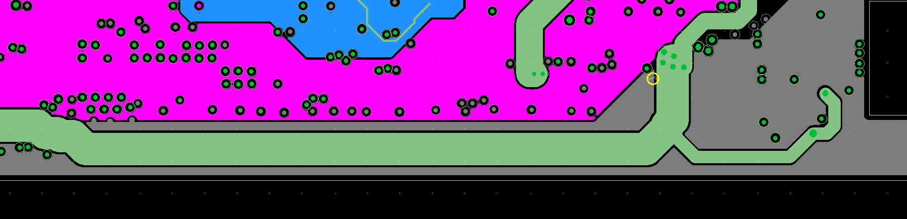
So now these pairs are on a parallel course from the middle of the board just up until they pass the PMIC. Now they have to line up in the Y direction with the ESD protection and the connector. But, going through a 45 degree bend, one track will now be shorter than the other, and that means that each pair (inter-pair) would have "skew". Now, that's fine if there was an opposite 45 degree bend within 15 mil (0.015 in) but there isn't... so it's necessary to add a small "wiggle" so that the 45 degree upwards straight has both tracks (on each pair) properly aligned. Then finally when they reach the VIAs (or the ESD protection), then another exactly-matching wiggle can be added to correct for the opposite-lock 45 degree turn. TX1 has to be a little bit odd: there are two sets of 45-followed-by-opposite-45 which we just have to live with: there's just not enough room otherwise.
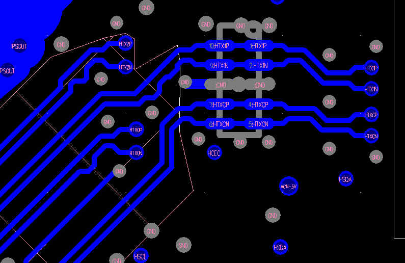
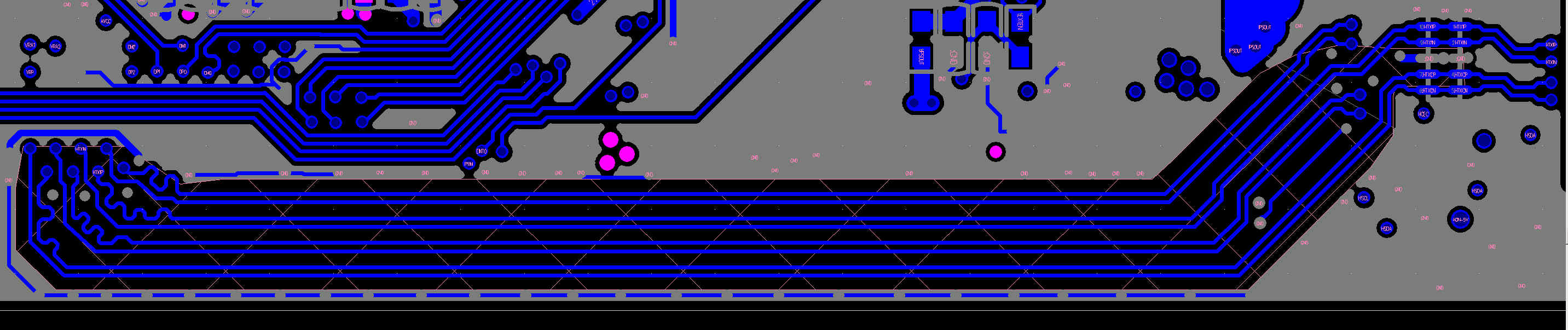
Two of the pairs then disappear up to Layer 1 (red), and the other two span out to the ESD protection on this side of the PCB, then cross over and finally come back up to meet the HDMI connector. Each section of each set of pairs at all times being to within 0.01 or 0.02 mil tolerance (skew). These last sections in particular being to 0.00 mil.
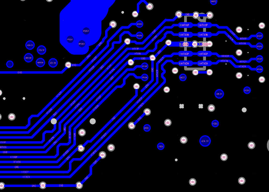
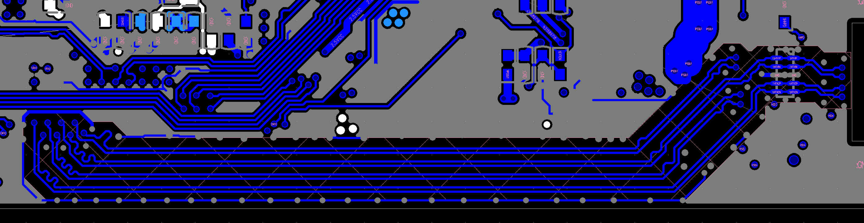
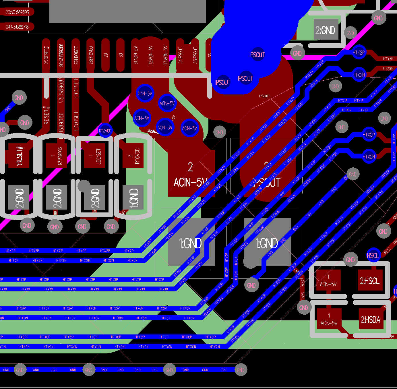
On the other side of the PCB is where it starts to get a little hairy. The two pairs (TX2 and TX0) which came up from ViAs: one of them has to take a wiggle (symmetrical tracks - look carefully!) whilst TX2 was also very carefully laid out (in the positioning of the VIAs) so that on this red side the tracks could be absolutely dead-straight.
Unfortunately, the ESD cannot be placed directly inline with the connector in order to have the tracks connecting it be symmetrical... not because of the ESD on this TOP side but because of the position of the one on the opposite side of the PCB! Why? because of the GND vias in between the two. If those VIAs are to be added (and they're important because otherwise Pin 7 on the Micro HDMI connector cannot be GND'ed properly) then these two ESD components need to be perfectly lined up.
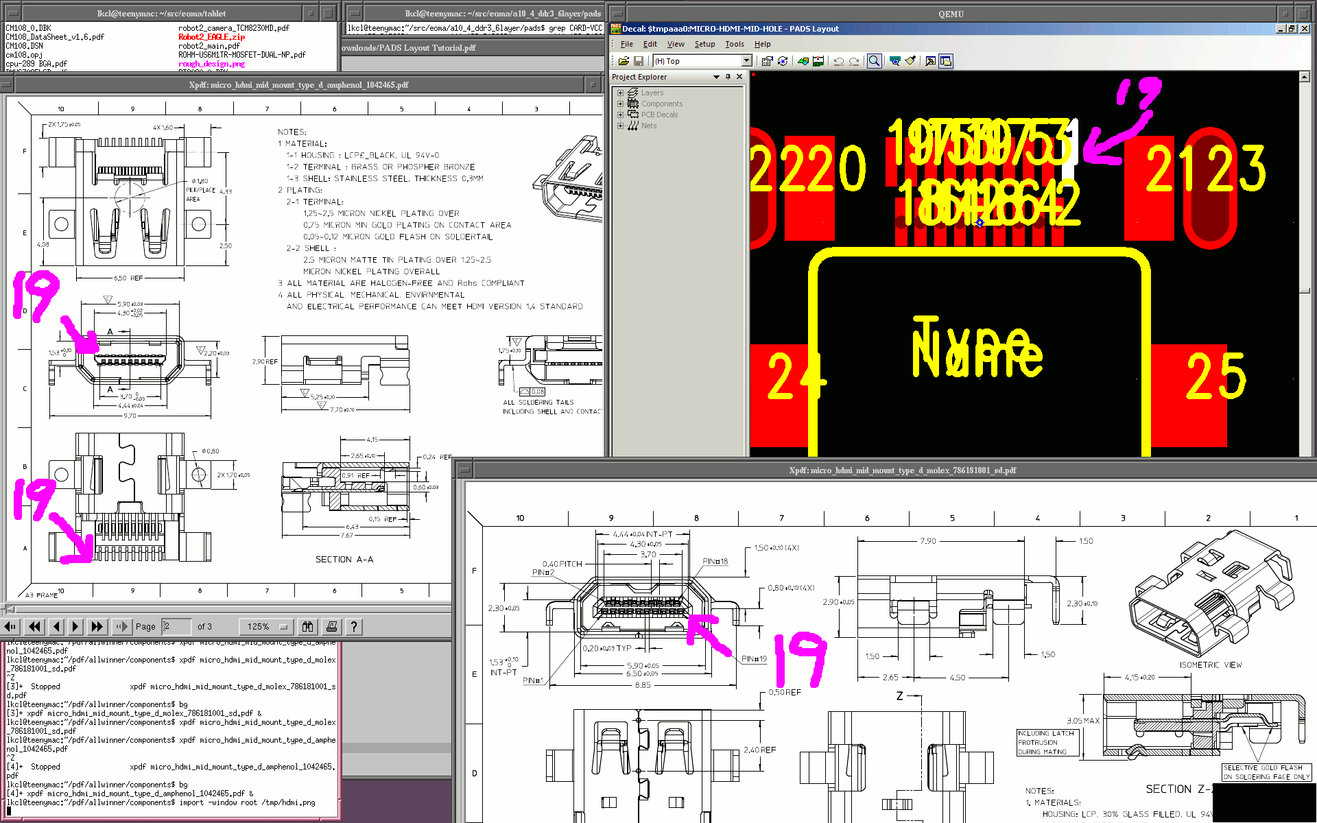
Finally we have the actual connector, which was the focus of the last report here. Those are 0402 VIAs (0.4mm ring, 0.2mm hole) and they're the cost-effective option. If you start using smaller than that, it's in to costly laser-drilling (even these 0.2mm holes are costly) and they won't fit in between the two rows of pins. Texas Instruments actually have a successful layout which does put the VIAs in between them but the clearances look to be really hair-rasing. This is all done on a 5 mil clearance, which is a good cost-effective design choice that is quite common.
The only problem with the VIAs being to the right of the connector is that they're (a) hard up against the edge of the PCB and (b) undergoing a 180 U-turn which is generally very very bad. However, in this particular case, the "saving grace" is that the pins with the exact same signal on them are directly above where the VIAs come out, which, it is guessed, results in little EM Radiation. Not only that but there is the metal (grounded) shield of the connector, which it is assumed will be in contact with the (metal, grounded) HDMI connector, thus providing a proper shield. Also each differential pin pair is surrounded, left right and either above or below by a GND pin: Micro-HDMI Type D has been deliberately designed to be this way.
So that's a very fast walkthrough of the dozen or so criteria that had to be satisfied in this extremely restricted space, to get 4 sets of 350mhz signals across a space of 40mm that's only around 8mm wide, staying only on two of the available layers and turning right-angles immediately and and and and...
... it has taken place on the available schedule of part-time people helping out, for which everyone will be extremely grateful, not just if it works but also for the fact that the discussion took place at all, and the archives now contain that knowledge for anyone wishing to research it and do their own high-speed differential pairs.
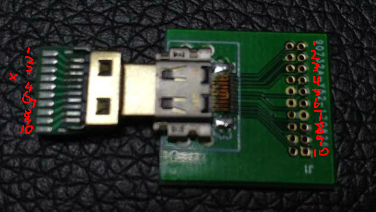
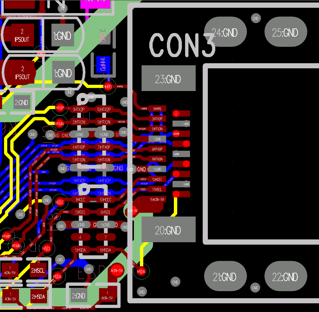
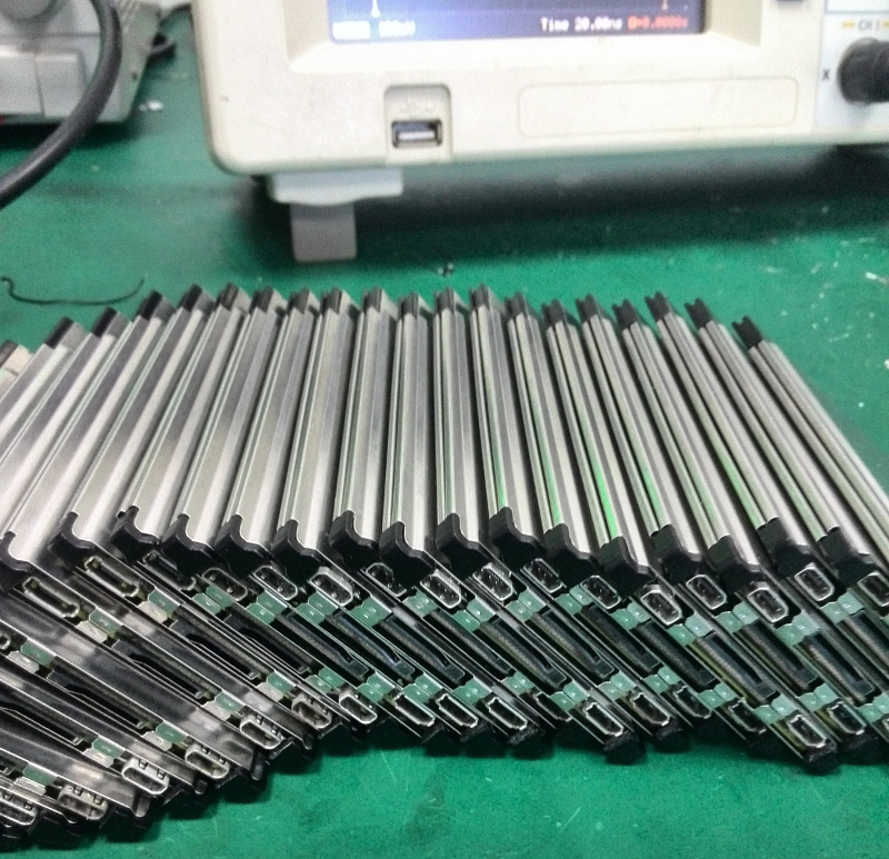
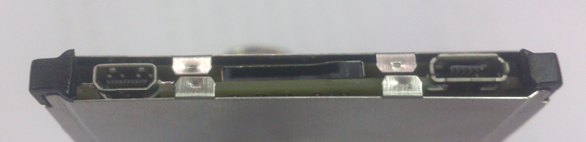
3 Jul 2017: EOMA68-A20 Revision 2.7.5: HDMI Connector Test Board
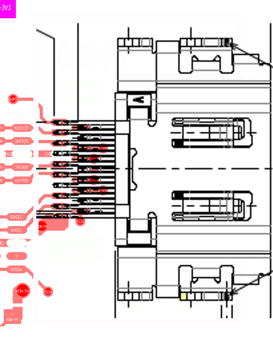
Before going ahead with Revision 2.7.5 it's essential to ensure that the JAE Micro-HDMI connector is production-ready and that the tracks and footprint are good. Kind offers of assistance in analysing the layout have been received, so these images are being published to help with that. The proposed current footprint has been overlaid with a copy of the datasheet's footprint, so that it can be confirmed as acceptable: the pins are 0.2mm wide and only 0.2mm apart. Also the differential pairs have been redone, widening the board by 0.8mm so that all four HDMI differential pairs can be placed on the same layer (bottom) including ground separation. A low-cost test board will be made to verify the footprint. This is the last round of pre-production prototyping that will be undertaken: if this does not work then Micro-HDMI will simply be dropped from the board.
15 Jun 2017: EOMA68-A20 Revision 2.7.4 PCBs
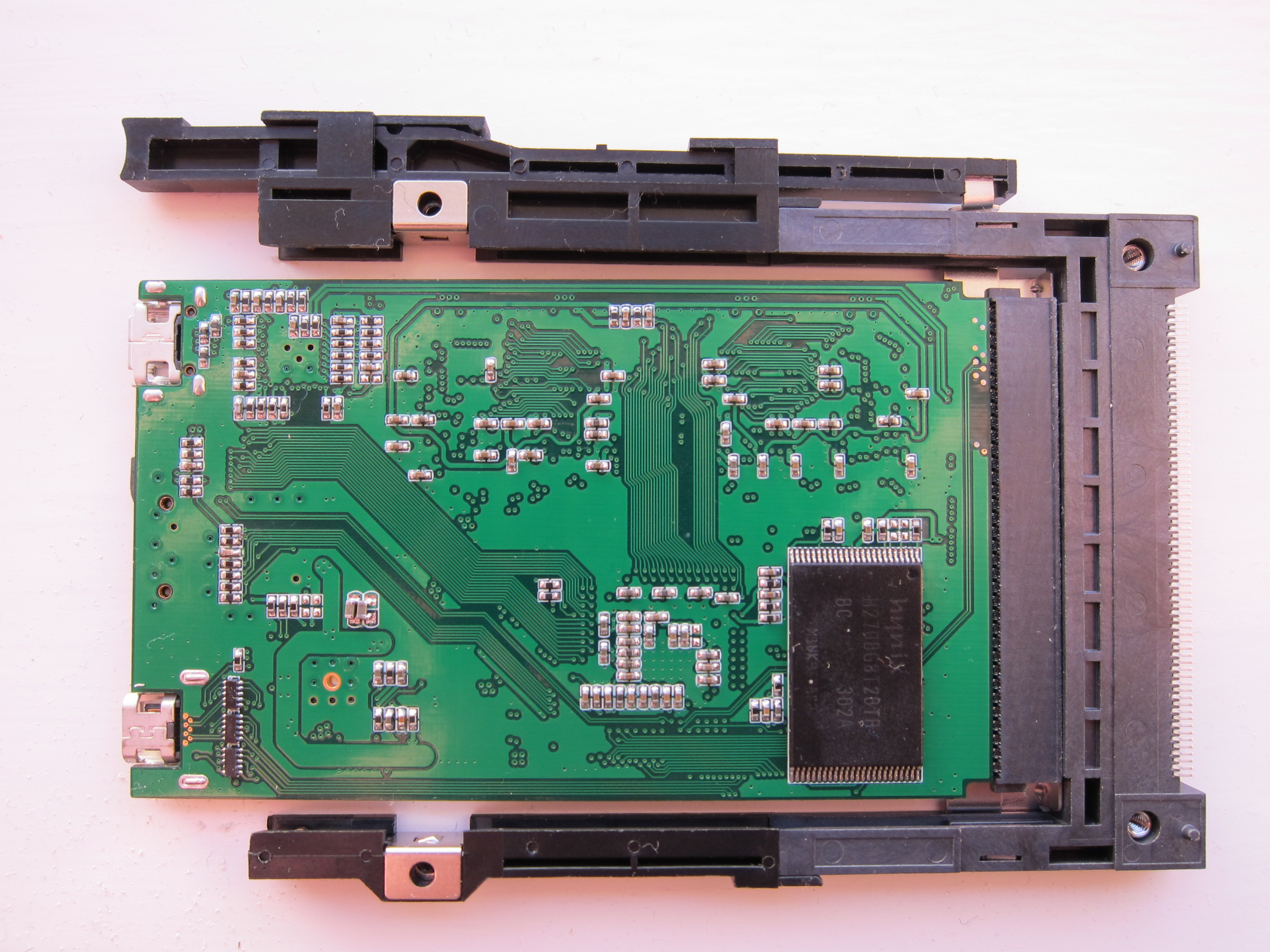
The 2.7.4 pre-production PCBs have come back from the factory: first sample tested works perfectly. However during the testing to establish suitability for production it was discovered that the JAE HDMI DC3 connector pads are so small that the VIAs underneath them are sucking the solder paste away. This needs to be solved before production begins. Ideas are being solicited for a (low-cost) test PCB so as not to have to have another $USD 2,000 round taking many weeks.
13 Oct 2016: EOMA68-A20 Revision 2.4 PCBs
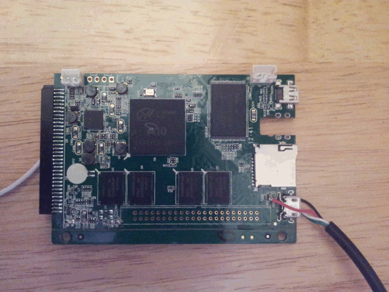
Mike is extremely busy with a deadline for this weekend but had time to take photos of the new EOMA68-A20 PCBs which he will be populating with 2GB of RAM soon. I am going to Shenzen next week, for the rest of the 30 day stay of the 2-entry visa, hopefully these will be ready by then and we can test them. Also the Microdesktop 1.4 is being done at the same time.
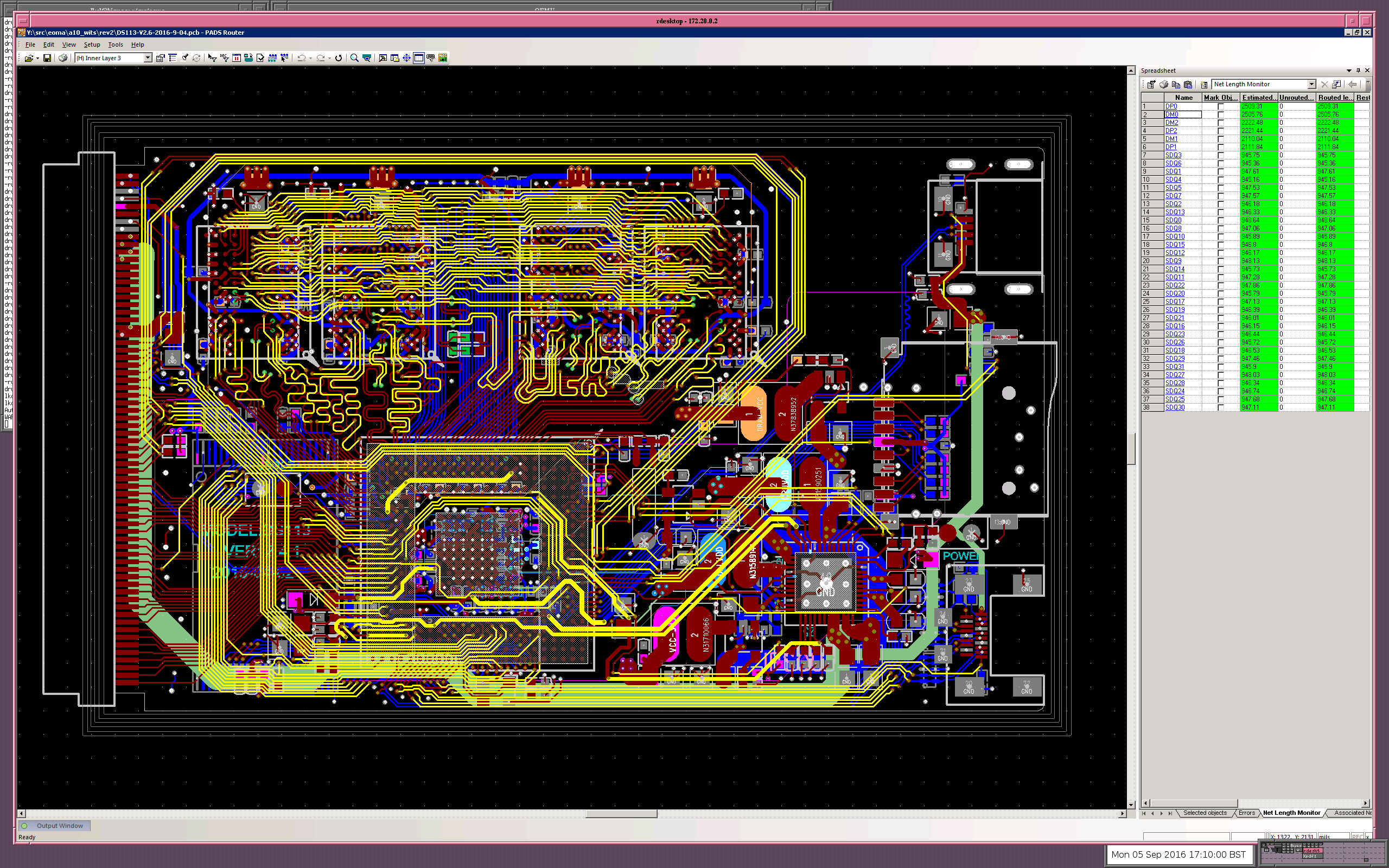
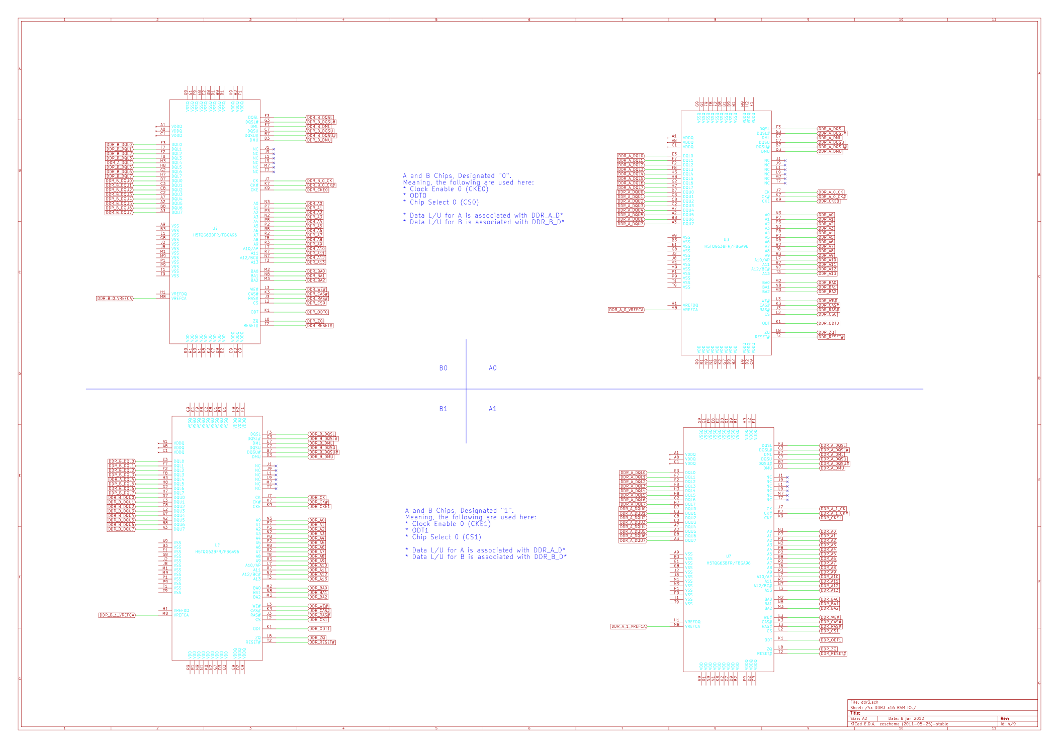
5 Sep 2016: Update to 2GB RAM DDR3 Routing
After the successful crowd-funding campaign work has begun to update the routing for the EOMA68-A20, adding an extra address line (SA15) which will allow the full 2GB RAM to be addressed. The Cubietruck schematics puzzlingly use four DDR3 x8 RAM ICs. However on close investigation it was discovered that this arrangement costs only $12, where two DDR3 x16 RAM ICs would cost $9 each for a total of $18! Therefore the plan to convert to 2 DDR3 x16 RAM ICs is abandoned in favour of keeping the original 4 DDR3 x8 RAM and simply adding the extra address line.
Sadly, much of Mr Xu's original and beautiful work, with arcs in use absolutely everywhere to produce something more akin to artwork than to a PCB layout, has been disrupted. However, the DDR3 data lines have not been touched (at all). On the right hand side of the picture below, all lengths are between 945 and 947 mil (thousandths of an inch). This is pretty incredible. DDR3 Address lines are less fussy for accuracy, however some effort has been made to get as close back to Mr Xu's work as possible, particularly adding back in the beautiful arcs on the DDR3 Clock differential pairs.
It is highly suspected that due to the quality of this work by Mr Xu, the EOMA68-A20 board could potentially run with 1333 or even 1600 Mhz DDR3 RAM. However, the power draw (which goes up as a square law) would increase over the rated 800mhz (around 350mA) by a factor of four if run at 1600mhz (to 1.4A). This is far too much for the AXP209 PMIC to handle, let alone the EOMA68 specification, given that the A20 uses 2.5 watts on its own, and the specification maxes out at 5.0 watts. Still, it is worth exploring to see if 1033 or 1333mhz works.
30 Oct 2014: Micro-Desktop and EOMA68-A20 running Debian 7.0 (Wheezy)
A lot has happened in the past few weeks, most of it on the Micro-Desktop news page. Here we show the Revision 2.2 Embedded Open Modular Architecture EOMA68-A20 CPU Card prototype working with the Micro-Desktop base unit. Boot-up is done using the Micro-Desktop's SD/MMC Card holder because that has been (intentionally) connected to the A20's "unbrickable" SD/MMC 0 slot. The demo shows the use of the VGA connector, which is not done using the A20's VGA RGB output wires but is instead done by a manual set of 6-bit A/D converters that take the A20's RGB/TTL LCD signals. Officially the EOMA-68 specification limits 5mm height CPU Cards to a maximum of 1280x800. The demo was with a 4:3 aspect ratio monitor so 1024x768 was selected.
Also shown working here is the lower of the two full-speed USB2 outputs (the other will have to wait for a tiny revision to the CPU Card, swapping the D+ and D- USB signals, which have been confirmed working... just not in the Micro-Desktop Board). Ethernet is also confirmed as operational, as is both Micro-SD Card slots, the RS232 / UART, and more.
10 Oct 2014: Revision 2.2 received
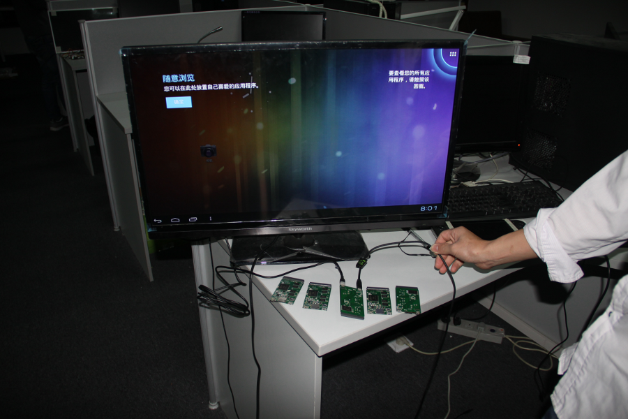
The Revision 2.2 boards (with 2Gb of RAM) were received after successful board bring-up confirmed that the CPU, PMIC, USB-OTG, DDR3 and NAND Flash are all operational. These are the major components. To be tested (once the Micro-Desktop boards arrive this week) are the Ethernet, two USB2 interfaces and the HDMI output. Once confirmed 100% the crowdfunding campaign can begin.
7 Oct 2013: All interfaces confirmed working
We've had confirmation for a few weeks that all interfaces are now working. There are a couple of modifications that would be nice to have made: most of these for a 2.5k run can be done with flying leads. We are now waiting for the MEB schematics to be made available so that they can be reviewed.
15 Jul 2013: First Batch (Group photo)
The A20 CPU Card first batch is now ready for shipping. They're to be picked up and then sent out shortly. Thank you to the 20 Free Software developers brave enough to take one of these at this very early phase. The picture below is one from a desk at Wits Tech's offices.
26 May 2013: CPU Cards running Debian 7.0 (Wheezy)
Thanks to help from Henrik Nordstrom who helped out significantly with the u-boot phase and in writing a USB FEX boot loader it is now possible to run Debian 7.0 Wheezy (armhf variant) on the first EOMA-68 CPU Card in the series, based on the A10 processor. Two demonstration videos have been created.
This first demonstration walks through the boot process, and shows how a 5V powered USB Hub has been connected to the EOMA-68 connector, as well as plugging in Micro-HDMI and powering from Micro-USB. Booting is done from a rather cheap and cheerful MicroSD Card from Asda's Supermarket.
This second video shows VLC (compiled with the CedarX modifications) running a full-screen HD Creative Commons video. Works perfectly. no glitches. Compilation was done natively using gcc-4.6.
29 Apr 2013: First sample pictures
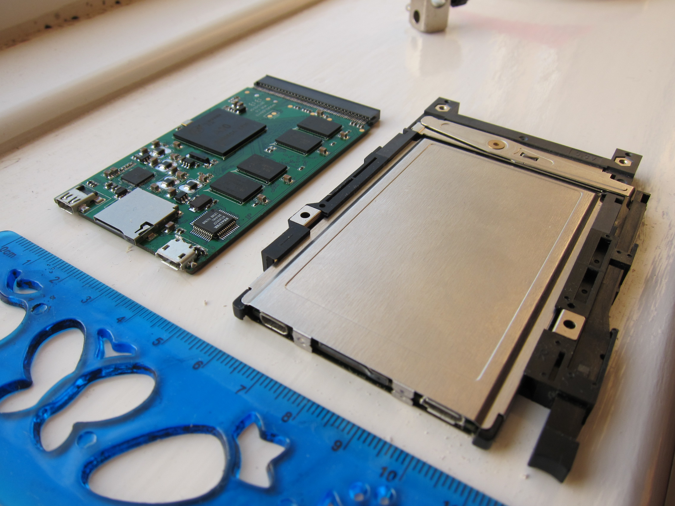
Last week Aaron's samples arrived, ahead of schedule. It's taken another week for two more to be shipped, and here they are! Photos below show them in an Amphenol PCMCIA socket, which is planned to be used in the 7in Flying Squirrel Tablet and many other products after that, including the 5in Hand-held Games Console and the Open Hardware Laptop. The A10 CPU Card can also take a Dual-Core ARM Cortex A7 Allwinner A20 processor with no modifications to the PCB.
12 Apr 2013: Working samples
Thanks to Wits-Tech, for sending us confirmation that the 5 samples are working. The next step is to get these out to critical clients as demo units and for testing to get the very first in the product family out the door as well, the 7in Flying Squirrel Tablet. In the mean-time, these can be sold as stand-alone products because they boot and are powered over USB-OTG and have HDMI out.
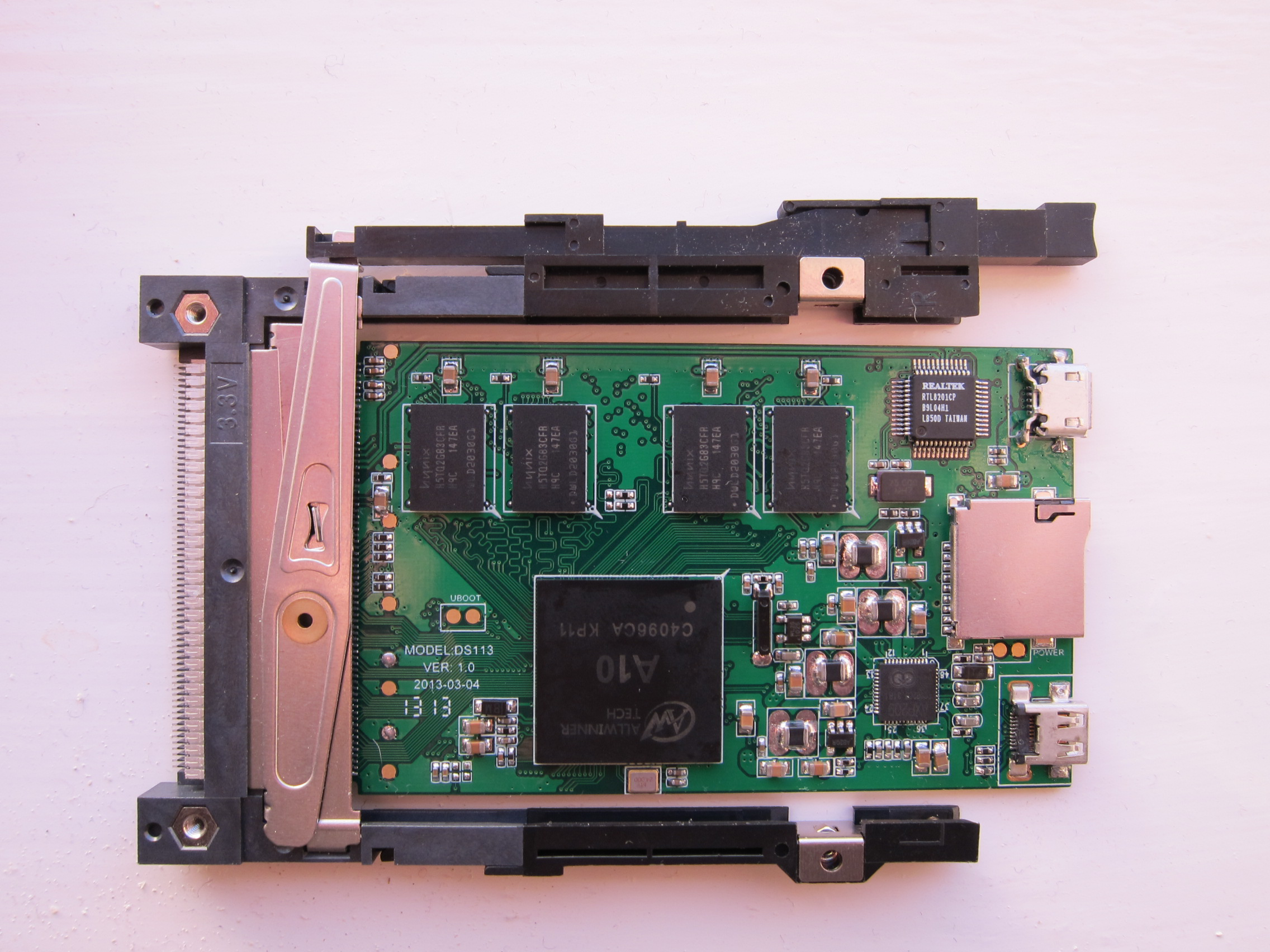
31 Mar 2013: Images of A10 PCB
Thanks to Wits-Tech, here's a screen-shot of the PCB that went to the factory for printing and component population 10 days ago: it should be back very shortly. We've arranged for 5 samples, one of which will have an A20 CPU. The best word to describe the layout is: beautiful. It's artwork. Mr Xul of Wits-Tech has clearly put considerable effort into ensuring that this PCB is not just properly laid out but tidy, with it.
The A10 CPU itself is to the left of the centre line, bottom. 4 DDR3 RAM ICs line the top, with the RT8021CP Ethernet PHY being in the top right, and the Micro-USB being to its right. It is a strange choice to have the ethernet lines running all the way to the corner and then all the way back to the EOMA68 connector, but this is a small board. AXP209 and other PMICs and discretes are in the bottom right quadrant; Micro-SD and Micro-HDMI are to their left.
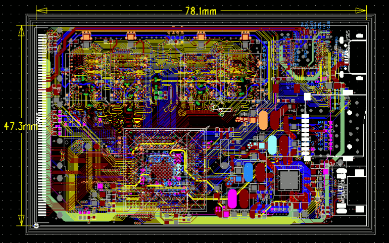
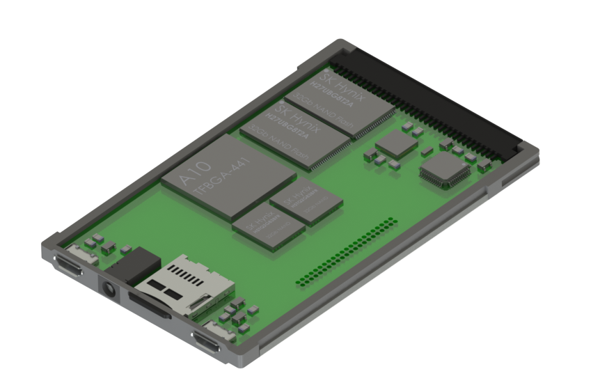
Here is a 3D rendering of the PCB, showing the major components.
23 Mar 2013: Litkconn show PCB and Case match up
Litkconn and Wits-Tech very kindly helped to confirm that the PCB size is now correct, and that it's practical to fit the PCB into the case. The plastic of P/N CH-PC-20 has been cut (the end removed) and a new one will need to be made. The current thinking is to create a 1.5mm thick aluminium stamped plate from sheet metal that, as part of the stamping process curls the ends inwards, to clip into the plastic edges left and right. It will also be glued (to the metal tabs) and then just for paranoia a sticky label wrapped around the whole lot, with the Serial Number on it. Clearance above the Micro-SD Card and Micro-HDMI is only 0.7mm: plastic isn't going to cut the mustard.
Other news: as can be seen, a test PCB went to Litkconn last week; following confirmation that the size is correct, samples have now been sent to the factory and will be populated with components within the next 10 days. The PCB design was actually completely re-done, hence it took slightly longer than strictly necessary. This included re-laying-out the Micro-HDMI and Micro-USB parts, and hilariously the PCB designer got them the wrong way round again. However due to the prior experience it was possible to check this before the PCB went out. It really is incredibly difficult to get Mid-Mount parts the right way round, especially on a datasheet that does not have numbering. Amphenol's Micro-HDMI had to be cross-references against a Molex equivalent, which allowed Pin 1 to be identified. Anyone wishing to have a hilarious time double-checking this, please feel free:
14 Dec 2012: First Revision EOMA-68 Sample CPU Card
Many thanks to Wits Tech for sending the sample all the way over from China, it arrived today.
6 Sep 2012: PCB design completed for EOMA-68 CPU Card
Many thanks to Wits Tech for completing the PCB design: the board layout and GERBER files are done. This brings the A10 EOMA-68 CPU Card one step closer to reality. The next stage is to get initial samples made up, the first script.fex created and a first boot completed.
Following on very very quickly from this, and driving a rather fast development schedule, is a commission from a client to convert an existing x86 laptop (1280x800) over to using the new A10 EOMA-68 CPU Card, and to provide 25 working prototypes for a Trade Show. Luckily, as the CPU Card is completely independent of the I/O Board, separate teams can focus on the development tasks.
Other news coverage:
28 Jul 2012: GPIO and Expansion Headers for EOMA-68 CPU Card
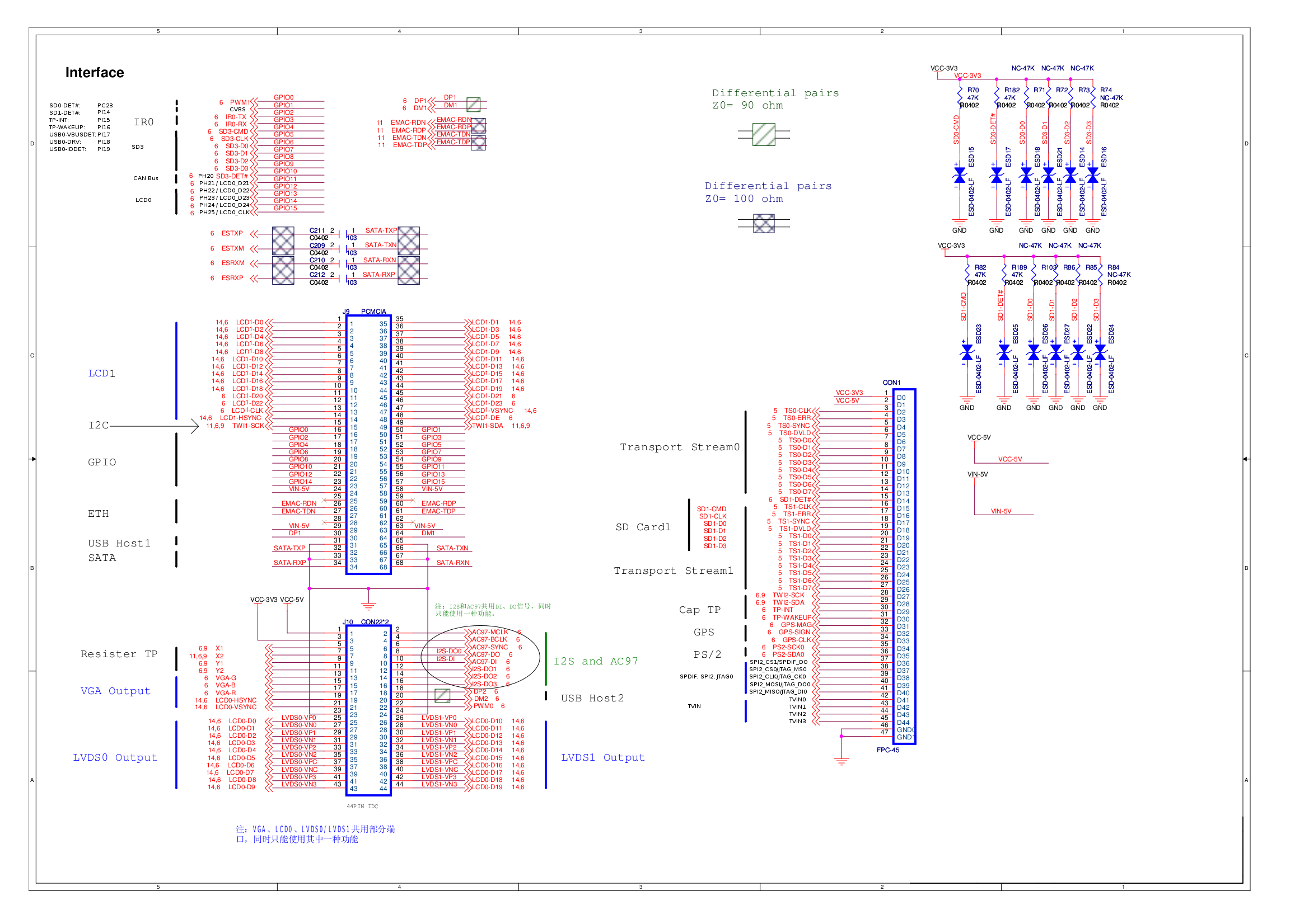
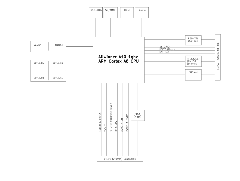
A rework of the GPIO and Expansion Headers for the first Qimod EOMA-68 CPU Card has been carried out. Almost all interfaces available of the Allwinner A10 CPU have been made available on the 55x85mm Credit-card-sized CPU Card, including both Transport Streams, SIM Card, PATA, the 24-pin Camera Interface, both 24-pin LCD Interfaces, VGA, Composite Video (CVBS), SPDIF, AC97, I2S, GPS, CAN-Bus, Infrared, and many more. This is in addition to the standard EOMA-68 Interfaces of Ethernet, I2C, SATA, LCD 24-pin RGB/TTL, USB2 and 16 GPIO pins.
The rework involved adding an extra optional 45-pin FPC, which is in addition to the optional 44-pin FPC. The ?orders page has been updated to reflect the full pinouts, as well as the finalised selection for the 16 EOMA-68 GPIO pins.
24 Jul 2012: Casework for EOMA-68 CPU Card
Titoma Design is delighted to be involved with the EOMA-68 project and has a preliminary design for the first EOMA-68 CPU Card, using the Allwinner A10 SoC. Titoma Design specialises in casework and full product design, and will be more than happy to assist clients to develop products based around the time and cost saving benefits of the EOMA-68 upgradeable design strategy.
09 Mar 2012: GSoC 2012 Application
Rhombus Tech is primarily an interface between the Free Software Community and factories in China. It makes sense therefore to apply as a GSoC 2012 Organisation. The first idea for a GSoC 2012 Project is quite a strategically important one: porting of OpenEC for use with an Embedded ARM Cortex M3.
OpenEC was used in the OLPC XO-1. The original firmware was proprietary, having been written by the Taiwanese Factory that manufactured the first XO-1s. This firmware had to be replaced under a Free Software License. The implications of that decision are that the Rhombus-Tech Project can use that code to create Embedded Firmware for other products - products which will have a reduced BOM and reduced cost, as a result.
So this is an opportunity for GSoC students to participate in an exciting project that will make quite a significant impact, as well.
18 Jan 2012: Update
Status report: a request for pricing the BOM for mass-volume has gone out to a large fully-automated factory in Shenzen. With Chinese New Year close, most of China is shutting down, with a few exceptional people still going (the owner of the large fully-automated factory being one of them). Progress on the schematics has helped narrow down the BOM. However, that was in KiCAD: the actual design which will need proper simulation especially of the DDR3 timings has to be done in ORCAD. As automated conversion from KiCAD to ORCAD is inconvenient, that will have to be done manually. Fortunately, given that Wits-Tech supplied ORCAD schematics for a basic tablet, this is less work.
Other news: the arm-netbooks mailing list is alive and kicking with further research on alternative processors (being documented in the evaluated cpus page). The challenge is to find a multi-core CPU that is affordable or otherwise desirable (i.e. modern) yet also has the full range of interfaces such as SATA-II, 10/100 Ethernet and RGB/TTL or LVDS. Many of the Cortex A9s examined in the past few days, such as the iMX6 or the A9600, are found to have LVDS and/or MIPI with no indication of whether they have RGB/TTL. The Nusmart 2816, which was announced as nearly available well over a year ago, is unfortunately now beginning to get some competition.
10 Jan 2012: ITWire News Article
Thank you to Sam for publishing an article about Rhombus Tech on ITWire.
8 Jan 2012: Overview Design
Schematics appear to be progressing rapidly - the devil however is always in the details. High-level decisions need to be taken at this point, however, particularly on which of the multiplexed functions are best put onto the 44-pin Expansion Header. It turns out that the Allwinner A10 has two RGB/TTL LCD interfaces, one of which can be multiplexed to dual-channel LVDS, and the other to IDE (PATA).
A deliberate decision has been made to place the PATA-multiplexed LCD interface onto the EOMA-68 connector, so that it is very clear that EOMA-68 is 24-pin RGB/TTL, not LVDS. The last thing that is needed is for motherboard manufacturers to take short-cuts with the standard, forcing all CPU cards to be more expensive by virtue of having to have on-board LVDS.
7 Jan 2012: DDR3 RAM PCB Design
After reviewing half a dozen DDR3 RAM documents, the absolute best one with the crucial advice needed was from Texas Instruments. From this, enough information was available to be able to make a decision to put in two banks (as if there were two DIMMs), one bank on the CS0/CK0/ODT0 lines and one on the CS1/CK1/ODT1 lines, and to place each pair of ICs in each bank onto 16-bit data lines. The DQS and DM lines are then associated with each 16-bit set of data lines (rather than being associated with each bank).
It would also be possible to lay out an 8-chip arrangement by having 8-bit RAM ICs: this is still under consideration in case 8 DDR3 x8 RAM ICs turn out to be lower cost than 4 DDR3 x16 ICs. However: with the chosen arrangement for now, 4 x16 DDR3 RAM ICs have to be chained together, with the DDR3 RAM controller automatically taking into account the different track lengths. In some ways this is fascinating but also a little scarey: DDR3 signals operate on a "fly-by" principle, where the read/write is delayed depending on how long the tracks are, to each IC. Amazing design concept.
2 Jan 2012: Starting PCB Design
Instead of waiting for the factory in China to finish their present client's work, 3 people have agreed to help initiate the development of the PCB Schematics. The process will be shortened by making use of the Evaluation Board Schematics: notes are being taken on its components here. A git repository containing KiCAD PCB libraries, modules and components has been established, called EOMA.
Bari from onelabs.com, and Jon Smirl, both have expertise in ORCAD, which allows for the complex CPU-DDR3 RAM traces to be resolved; Michelle has expertise in KiCAD and is used to doing CPU-DDR3 traces to within 0.020in by hand (!). Luke Leighton is acting as the general dogsbody and sucker for trawling through available resources and datasheets in order to create pinouts and parts.
The Factory in Shenzen is presently closed for the New Year: we will re-establish contact with them as soon as possible, and by then will have something to pass over to them, to help accelerate the development.
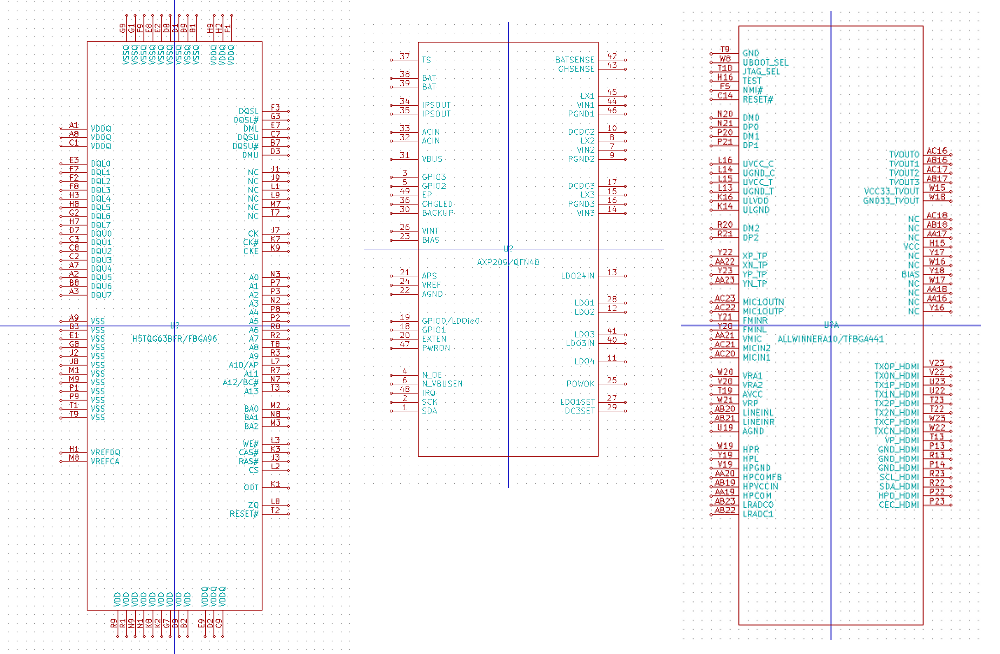
3 parts have been completed in KiCAD so far: the Allwinner A10 CPU, the PMIC AXP209 and the Hynix DDR3 RAM 2gb x16 RAM IC H5TQ2G8(6)3BFR(Rev1.8). Pinouts below:
30 Dec 2011: Allwinner to release a $4.99 ARM Cortex A8
A newsreport on micdigi.com has been found, which reports that Allwinner is to release a CPU in the A1x family that will be $4.99 in mass-volume. To achieve such a target, the CPU's packaging has to be very small, and the number of pins reduced from the 400 pins of the A10 down to 300 or even less. It will be very interesting to see what Allwinner come up with.
19 Dec 2011: Factory delighted with preorders
I contacted the factory in China, told them about the preorders page, and they were absolutely delighted, you could tell they were proud and pleased to be involved. James (the Factory Owner) has to focus on a customer order this week: after that he will be full-time on creating the PCMCIA-sized CPU board.
15 Dec 2011: discussion with Factory
A discussion took place today with the factory regarding PCB layout. Of paramount importance to them is to ensure that the resultant PCB will be useful for a number of mass-volume purposes. The unspoken implication is that if that same PCB happens to be EOMA-68-compliant, they would not mind designing it to suit RHT's goals, even though those goals would also benefit the Factory as well!
So, taking the Allwinner Reference Board, a basic reworking was done cut/paste style to prove that all the components needed for a low-cost board would fit into an 85mm x 55mm space. For scale, the 44-pin connector's pins are 2.0mm apart. The result can be seen, here:
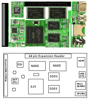
The key to independent use for the Factory is the 44-pin connector, on which strategically-picked interfaces can be placed, such as the Camera Interface, TV-out, the spare USB2, the Resistive Touch Controller, extra SD/MMC interfaces and so on. By a happy coincidence, many of these additional interfaces will be of use to Engineers and Software (Libre) Developers as well.
The only unusual ICs which require some explanation are the inclusion of a Power Management IC (the AXP209) and the Ethernet IC, which is an RALink RTL8201CP. The Ethernet IC is required because the EOMA-68 specification requires Ethernet suitable for direct connection to an RJ-45 connector, not MII. Other than that, there is just enough space to fit two DDR3 RAM ICs and two NAND ICs, without having to use the other side of the PCB.
As this is a preliminary layout, it may be possible to squeeze things further, in particular, fitting a second 44-pin connector for further expansion purposes. For example, the A10 has an IDE interface (PATA), the same pins can be switched over to a 2nd LCD RGB/TTL Interface.